- 您现在的位置:买卖IC网 > PDF目录97869 > DS2433X (DALLAS SEMICONDUCTOR) 4K X 1 1-WIRE SERIAL EEPROM, UUC2 PDF资料下载
参数资料
| 型号: | DS2433X |
| 厂商: | DALLAS SEMICONDUCTOR |
| 元件分类: | Programmable ROM |
| 英文描述: | 4K X 1 1-WIRE SERIAL EEPROM, UUC2 |
| 封装: | DIE |
| 文件页数: | 7/19页 |
| 文件大小: | 457K |
| 代理商: | DS2433X |
DS2433
15 of 19
1-WIRE SIGNALING
The DS2433 requires strict protocols to insure data integrity. The protocol consists of four types of
signaling on one line: Reset Sequence with Reset Pulse and Presence Pulse, Write 0, Write 1 and Read
Data.
All these signals except Presence Pulse are initiated by the bus master.
The DS2433 can
communicate at two different speeds, regular speed and Overdrive Speed. If not explicitly set into the
overdrive mode, the DS2433 will communicate at regular speed. While in Overdrive Mode the fast
timing applies to all wave forms.
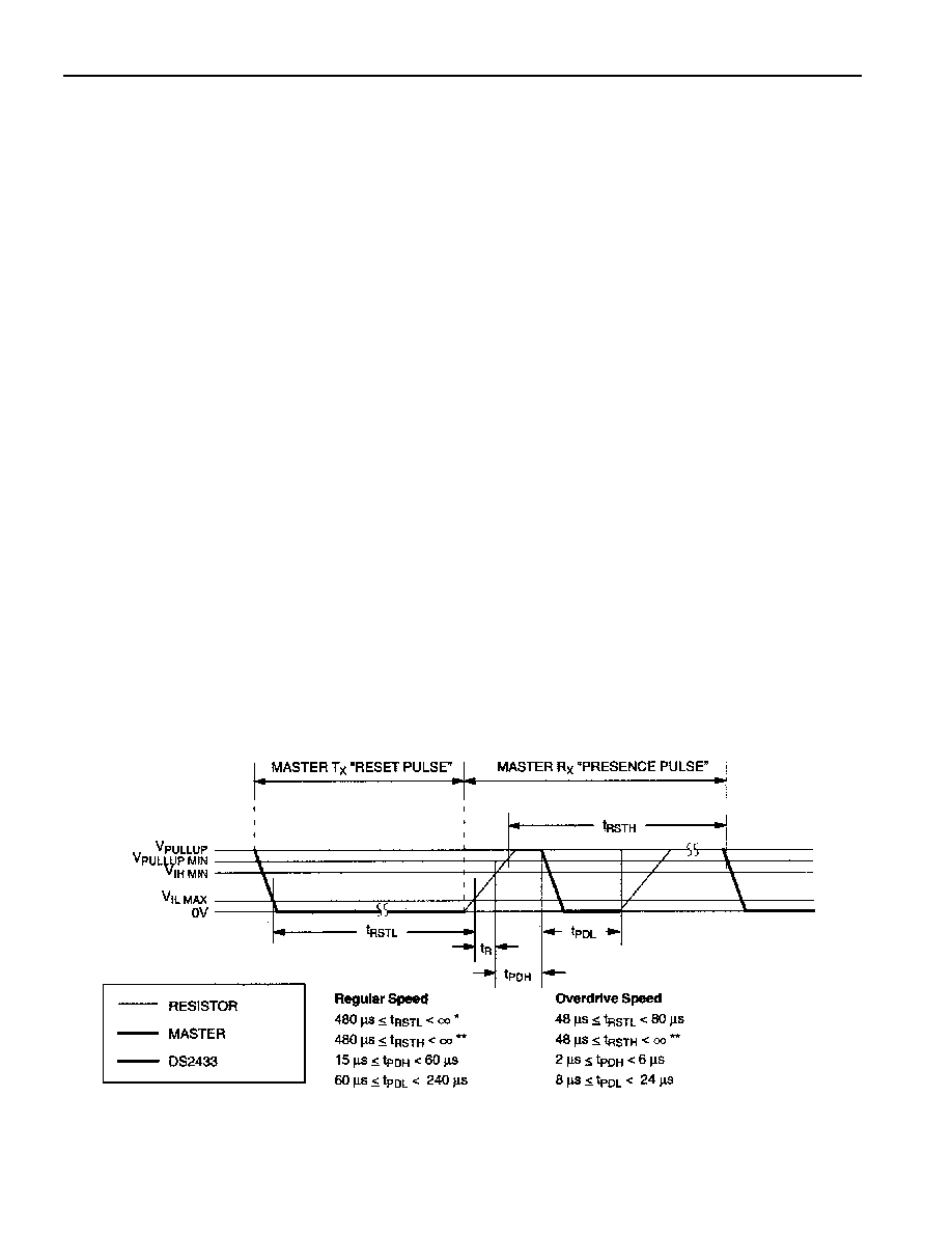
The initialization sequence required to begin any communication with the DS2433 is shown in Figure 10.
A Reset Pulse followed by a Presence Pulse indicates the DS2433 is ready to send or receive data given
the correct ROM command and memory function command. The bus master transmits (TX) a Reset
Pulse (tRSTL, minimum 480
s at regular speed, 48 s at Overdrive Speed). The bus master then releases
the line and goes into receive mode (RX). The 1-Wire bus is pulled to a high state via the pullup resistor.
After detecting the rising edge on the data pin, the DS2433 waits (tPDH, 15-60
s at regular speed, 2-6 s
at Overdrive speed) and then transmits the Presence Pulse (tPDL, 60-240
s at regular speed, 8-24 s at
Overdrive Speed).
A Reset Pulse of 480
s or longer will exit the Overdrive Mode returning the device to regular speed. If
the DS2433 is in Overdrive Mode and the Reset Pulse is no longer than 80
s the device will remain in
Overdrive Mode.
READ/WRITE TIME SLOTS
The definitions of write and read time slots are illustrated in Figure 11. All time slots are initiated by the
master driving the data line low. The falling edge of the data line synchronizes the DS2433 to the master
by triggering a delay circuit in the DS2433. During write time slots, the delay circuit determines when
the DS2433 will sample the data line. For a read data time slot, if a “0” is to be transmitted, the delay
circuit determines how long the DS2433 will hold the data line low overriding the 1 generated by the
master. If the data bit is a “1”, the device will leave the read data time slot unchanged.
INITIALIZATION PROCEDURE RESET AND PRESENCE PULSES Figure 10
*In order not to mask interrupt signalling by other devices on the 1-Wire bus, tRSTL + tR should always be less than 960 s.
** Includes recovery time.
相关PDF资料 |
PDF描述 |
|---|---|
| DS2433S | 512 X 8 1-WIRE SERIAL EEPROM, PDSO8 |
| DS2434S | SPECIALTY MEMORY CIRCUIT, PDSO16 |
| DS2434 | SPECIALTY MEMORY CIRCUIT, PBCY3 |
| DS2435 | SPECIALTY MEMORY CIRCUIT, PBCY3 |
| DS2436B | SPECIALTY MEMORY CIRCUIT, PBCY3 |
相关代理商/技术参数 |
参数描述 |
|---|---|
| 532HB622M080BG | 制造商:SILABS 制造商全称:SILABS 功能描述:DUAL FREQUENCY XO (10 MHZ TO 1.4 GHZ) |
| 532HB622M080BGR | 制造商:SILABS 制造商全称:SILABS 功能描述:DUAL FREQUENCY XO (10 MHZ TO 1.4 GHZ) |
| 532HEX | 制造商:Belden Inc 功能描述: |
| 532JA622M080BG | 制造商:SILABS 制造商全称:SILABS 功能描述:DUAL FREQUENCY XO (10 MHZ TO 1.4 GHZ) |
| 532JA622M080BGR | 制造商:SILABS 制造商全称:SILABS 功能描述:DUAL FREQUENCY XO (10 MHZ TO 1.4 GHZ) |
发布紧急采购,3分钟左右您将得到回复。