参数资料
| 型号: | AD620BRZ-RL |
| 厂商: | Analog Devices Inc |
| 文件页数: | 11/21页 |
| 文件大小: | 0K |
| 描述: | IC AMP INST LP LN 18MA 8SOIC |
| 设计资源: | Low Cost Programmable Gain Instrumentation Amplifier Circuit Using ADG1611 and AD620 (CN0146) |
| 标准包装: | 2,500 |
| 放大器类型: | 仪表 |
| 电路数: | 1 |
| 转换速率: | 1.2 V/µs |
| -3db带宽: | 1MHz |
| 电流 - 输入偏压: | 500pA |
| 电压 - 输入偏移: | 15µV |
| 电流 - 电源: | 900µA |
| 电流 - 输出 / 通道: | 18mA |
| 电压 - 电源,单路/双路(±): | 4.6 V ~ 36 V,±2.3 V ~ 18 V |
| 工作温度: | -40°C ~ 85°C |
| 安装类型: | 表面贴装 |
| 封装/外壳: | 8-SOIC(0.154",3.90mm 宽) |
| 供应商设备封装: | 8-SO |
| 包装: | 带卷 (TR) |
AD620
Rev. H | Page 18 of 20
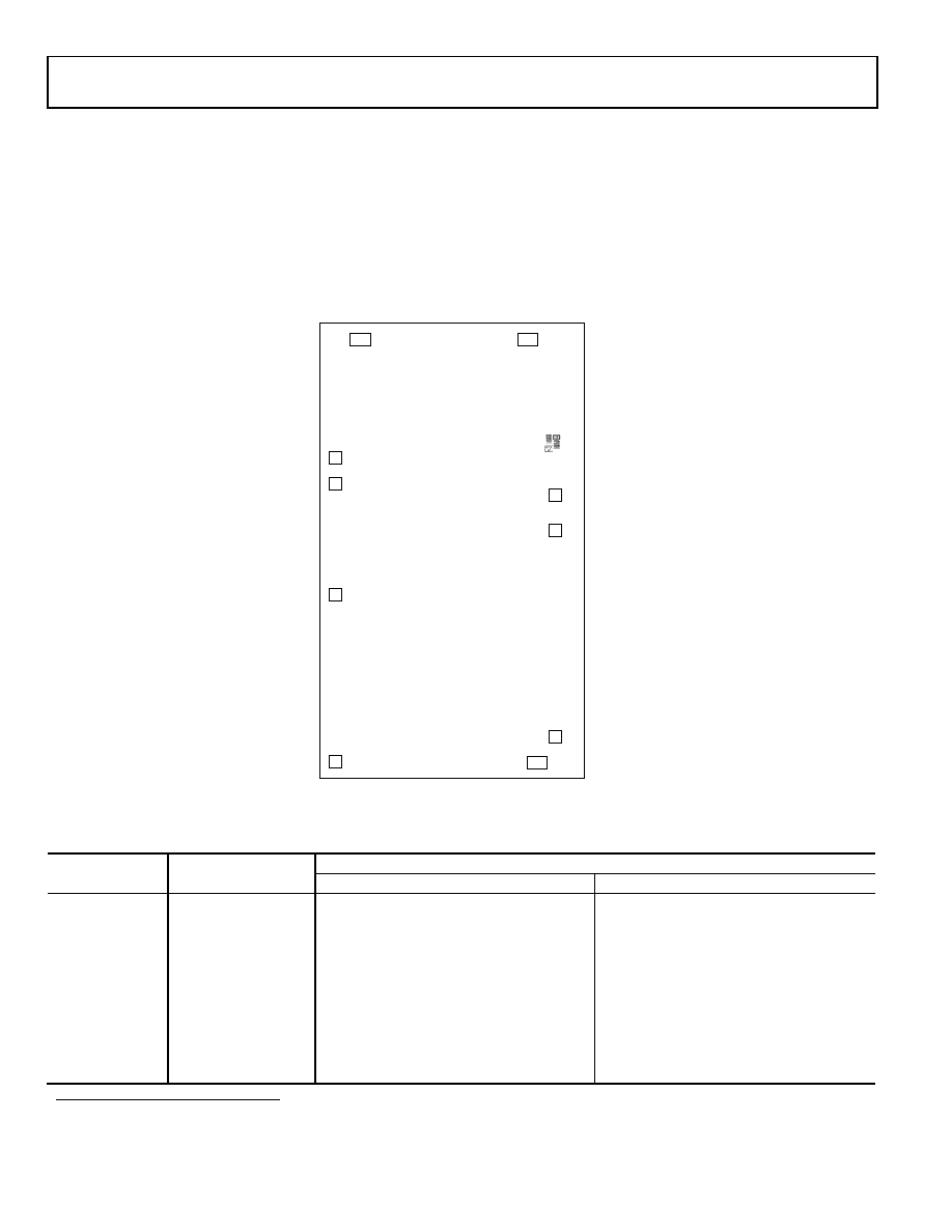
AD620ACHIPS INFORMATION
Die size: 1803 μm × 3175 μm
Die thickness: 483 μm
Bond Pad Metal: 1% Copper Doped Aluminum
To minimize gain errors introduced by the bond wires, use Kelvin connections between the chip and the gain resistor, RG, by connecting
Pad 1A and Pad 1B in parallel to one end of RG and Pad 8A and Pad 8B in parallel to the other end of RG. For unity gain applications
where RG is not required, Pad 1A and Pad 1B must be bonded together as well as the Pad 8A and Pad 8B.
1A
1B
2
3
4
5
6
7
8A
8B
LOGO
00
775-
0-
053
Figure 49. Bond Pad Diagram
Table 6. Bond Pad Information
Pad Coordinates1
Pad No.
Mnemonic
X (μm)
Y (μm)
1A
RG
623
+1424
1B
RG
789
+628
2
IN
790
+453
3
+IN
790
294
4
VS
788
1419
5
REF
+570
1429
6
OUTPUT
+693
1254
7
+VS
+693
+139
8A
RG
+505
+1423
8B
RG
+693
+372
1 The pad coordinates indicate the center of each pad, referenced to the center of the die. The die orientation is indicated by the logo, as shown in Figure 49.
相关PDF资料 |
PDF描述 |
|---|---|
| 0234003.MXBP | FUSE 5X20 C/CODE M 3A/250V |
| AD629BR-REEL7 | IC AMP DIFF 25MA LDRIFT 8SOIC |
| TSM-105-01-L-DV | CONN HEADER 10POS .100" DBL SMD |
| AD629BR-REEL | IC AMP DIFF 25MA LDRIFT 8SOIC |
| MTMM-106-09-T-D-090 | CONN HEADER 12POS 2MM DL TIN |
相关代理商/技术参数 |
参数描述 |
|---|---|
| 6680005578829 | 制造商: 功能描述: 制造商:undefined 功能描述: |
| 6680008268807 | 制造商: 功能描述: 制造商:undefined 功能描述: |
| 6680-00-882-0965 | 制造商: 功能描述: 制造商:undefined 功能描述: |
| 6680008912796 | 制造商: 功能描述: 制造商:undefined 功能描述: |
| 6680009296667 | 制造商: 功能描述: 制造商:undefined 功能描述: |
发布紧急采购,3分钟左右您将得到回复。