- 您现在的位置:买卖IC网 > PDF目录379542 > A54SX08A-2CQ208 (Electronic Theatre Controls, Inc.) SX-A Family FPGAs PDF资料下载
参数资料
| 型号: | A54SX08A-2CQ208 |
| 厂商: | Electronic Theatre Controls, Inc. |
| 元件分类: | FPGA |
| 英文描述: | SX-A Family FPGAs |
| 中文描述: | 的SX - A系列FPGA的 |
| 文件页数: | 37/108页 |
| 文件大小: | 720K |
| 代理商: | A54SX08A-2CQ208 |
第1页第2页第3页第4页第5页第6页第7页第8页第9页第10页第11页第12页第13页第14页第15页第16页第17页第18页第19页第20页第21页第22页第23页第24页第25页第26页第27页第28页第29页第30页第31页第32页第33页第34页第35页第36页当前第37页第38页第39页第40页第41页第42页第43页第44页第45页第46页第47页第48页第49页第50页第51页第52页第53页第54页第55页第56页第57页第58页第59页第60页第61页第62页第63页第64页第65页第66页第67页第68页第69页第70页第71页第72页第73页第74页第75页第76页第77页第78页第79页第80页第81页第82页第83页第84页第85页第86页第87页第88页第89页第90页第91页第92页第93页第94页第95页第96页第97页第98页第99页第100页第101页第102页第103页第104页第105页第106页第107页第108页
SX-A Family FPGAs
v5.1
2-17
Timing Characteristics
Timing characteristics for SX-A devices fall into three
categories: family-dependent, device-dependent, and
design-dependent. The input and output buffer
characteristics are common to all SX-A family members.
Internal routing delays are device-dependent. Design
dependency means actual delays are not determined
until after placement and routing of the user’s design are
complete. The timing characteristics listed in this
datasheet represent sample timing numbers of the SX-A
devices. Design-specific delay values may be determined
by using Timer or performing simulation after successful
place-and-route with the Designer software.
Critical Nets and Typical Nets
Propagation delays are expressed only for typical nets,
which are used for initial design performance evaluation.
Critical net delays can then be applied to the most
timing-critical paths. Critical nets are determined by net
property assignment prior to placement and routing. Up
to 6 percent of the nets in a design may be designated as
critical, while 90 percent of the nets in a design are
typical.
Long Tracks
Some nets in the design use long tracks. Long tracks are
special routing resources that span multiple rows,
columns, or modules. Long tracks employ three to five
antifuse connections. This increases capacitance and
resistance, resulting in longer net delays for macros
connected to long tracks. Typically, up to 6 percent of
nets in a fully utilized device require long tracks. Long
tracks contribute approximately 4 ns to 8.4 ns delay. This
additional delay is represented statistically in higher
fanout routing delays.
Timing Derating
SX-A devices are manufactured with a CMOS process.
Therefore, device performance varies according to
temperature, voltage, and process changes. Minimum
timing parameters reflect maximum operating voltage,
minimum
operating
temperature,
processing.
Maximum
timing
minimum operating voltage, maximum operating
temperature, and worst-case processing.
and
best-case
reflect
parameters
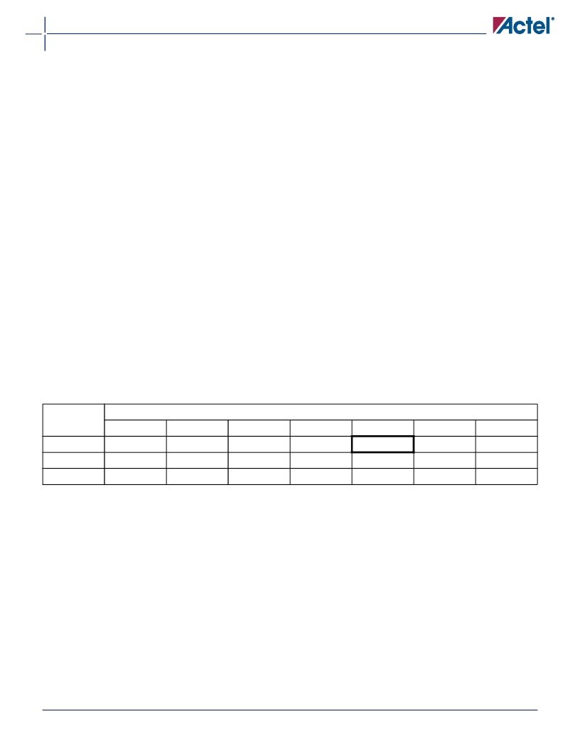
Temperature and Voltage Derating Factors
Table 2-13
Temperature and Voltage Derating Factors
(Normalized to Worst-Case Commercial, T
J
= 70
°
C, V
CCA
= 2.25 V)
V
CCA
Junction Temperature (T
J
)
0°C
25°C
–55°C
–40°C
70°C
85°C
125°C
2.250 V
0.79
0.80
0.87
0.89
1.00
1.04
1.14
2.500 V
0.74
0.75
0.82
0.83
0.94
0.97
1.07
2.750 V
0.68
0.69
0.75
0.77
0.87
0.90
0.99
相关PDF资料 |
PDF描述 |
|---|---|
| A54SX16A-2CQ208 | SX-A Family FPGAs |
| A54SX72A-2CQ208 | SX-A Family FPGAs |
| A54SX32A-2CQ208 | SX-A Family FPGAs |
| A54SX08A-2CQ208A | SX-A Family FPGAs |
| A54SX16A-2CQ208A | SX-A Family FPGAs |
相关代理商/技术参数 |
参数描述 |
|---|---|
| A54SX08A-2CQ208A | 制造商:未知厂家 制造商全称:未知厂家 功能描述:SX-A Family FPGAs |
| A54SX08A-2CQ208B | 制造商:未知厂家 制造商全称:未知厂家 功能描述:SX-A Family FPGAs |
| A54SX08A-2CQ208I | 制造商:未知厂家 制造商全称:未知厂家 功能描述:SX-A Family FPGAs |
| A54SX08A-2CQ208M | 制造商:未知厂家 制造商全称:未知厂家 功能描述:SX-A Family FPGAs |
| A54SX08A-2FG144 | 功能描述:IC FPGA SX 12K GATES 144-FBGA RoHS:否 类别:集成电路 (IC) >> 嵌入式 - FPGA(现场可编程门阵列) 系列:SX-A 标准包装:90 系列:ProASIC3 LAB/CLB数:- 逻辑元件/单元数:- RAM 位总计:36864 输入/输出数:157 门数:250000 电源电压:1.425 V ~ 1.575 V 安装类型:表面贴装 工作温度:-40°C ~ 125°C 封装/外壳:256-LBGA 供应商设备封装:256-FPBGA(17x17) |
发布紧急采购,3分钟左右您将得到回复。