- 您现在的位置:买卖IC网 > PDF目录19389 > ADSP-BF544BBCZ-4A (Analog Devices Inc)IC CCD SIGNAL PROCESSOR 400BGA PDF资料下载
参数资料
| 型号: | ADSP-BF544BBCZ-4A |
| 厂商: | Analog Devices Inc |
| 文件页数: | 10/100页 |
| 文件大小: | 0K |
| 描述: | IC CCD SIGNAL PROCESSOR 400BGA |
| 标准包装: | 1 |
| 系列: | Blackfin® |
| 类型: | 定点 |
| 接口: | CAN,SPI,SSP,TWI,UART |
| 时钟速率: | 400MHz |
| 非易失内存: | 外部 |
| 芯片上RAM: | 196kB |
| 电压 - 输入/输出: | 2.50V,3.30V |
| 电压 - 核心: | 1.25V |
| 工作温度: | -40°C ~ 85°C |
| 安装类型: | 表面贴装 |
| 封装/外壳: | 400-LFBGA,CSPBGA |
| 供应商设备封装: | 400-CSPBGA(17x17) |
| 包装: | 托盘 |
第1页第2页第3页第4页第5页第6页第7页第8页第9页当前第10页第11页第12页第13页第14页第15页第16页第17页第18页第19页第20页第21页第22页第23页第24页第25页第26页第27页第28页第29页第30页第31页第32页第33页第34页第35页第36页第37页第38页第39页第40页第41页第42页第43页第44页第45页第46页第47页第48页第49页第50页第51页第52页第53页第54页第55页第56页第57页第58页第59页第60页第61页第62页第63页第64页第65页第66页第67页第68页第69页第70页第71页第72页第73页第74页第75页第76页第77页第78页第79页第80页第81页第82页第83页第84页第85页第86页第87页第88页第89页第90页第91页第92页第93页第94页第95页第96页第97页第98页第99页第100页
ADSP-BF542/ADSP-BF544/ADSP-BF547/ADSP-BF548/ADSP-BF549
Rev. C
|
Page 17 of 100
|
February 2010
Sleep Operating Mode—High Dynamic Power Savings
The sleep mode reduces dynamic power dissipation by disabling
the clock to the processor core (CCLK). The PLL and system
clock (SCLK), however, continue to operate in this mode. Typi-
cally an external event or RTC activity will wake up the
processor. In the sleep mode, assertion of a wakeup event
enabled in the SIC_IWRx register causes the processor to sense
the value of the BYPASS bit in the PLL control register
(PLL_CTL). If BYPASS is disabled, the processor transitions to
the full on mode. If BYPASS is enabled, the processor transi-
tions to the active mode.
In the sleep mode, system DMA access to L1 memory is not
supported.
Deep Sleep Operating Mode—Maximum Dynamic Power
Savings
The deep sleep mode maximizes dynamic power savings by dis-
abling the clocks to the processor core (CCLK) and to all
synchronous peripherals (SCLK). Asynchronous peripherals,
such as the RTC, may still be running but will not be able to
access internal resources or external memory. This
powered-down mode can only be exited by assertion of the reset
interrupt (RESET) or by an asynchronous interrupt generated
by the RTC. In deep sleep mode, an asynchronous RTC inter-
rupt causes the processor to transition to the active mode.
Assertion of RESET while in deep sleep mode causes the proces-
sor to transition to the full on mode.
Hibernate State—Maximum Static Power Savings
The hibernate state maximizes static power savings by disabling
the voltage and clocks to the processor core (CCLK) and to all
the synchronous peripherals (SCLK). The internal voltage regu-
lator for the processor can be shut off by using the
bfrom_SysControl() function in the on-chip ROM. This sets the
internal power supply voltage (VDDINT) to 0 V to provide the
greatest power savings mode. Any critical information stored
internally (memory contents, register contents, and so on) must
be written to a non-volatile storage device prior to removing
power if the processor state is to be preserved.
Since VDDEXT is still supplied in this mode, all of the external
pins three-state, unless otherwise specified. This allows other
devices that may be connected to the processor to have power
still applied without drawing unwanted current.
The internal supply regulator can be woken up by CAN, by the
MXVR, by the keypad, by the up/down counter, by the USB,
and by some GPIO pins. It can also be woken up by a real-time
clock wakeup event or by asserting the RESET pin. Waking up
from hibernate state initiates the hardware reset sequence.
With the exception of the VR_CTL and the RTC registers, all
internal registers and memories lose their content in hibernate
state. State variables may be held in external SRAM or DDR
memory.
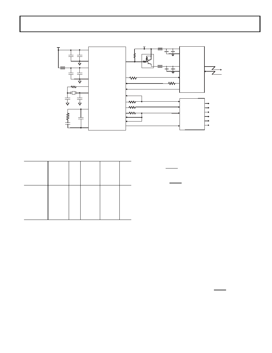
Figure 5. MXVR MOST Connection
600Z
MLF_M
MOST
NETWORK
AUDIO
CHANNELS
GNDMP
VDDMP
MOST FOT
TXVCC
TX_DATA
RX_DATA
STATUS
AUDIO DAC
27
R1
330
C1
0.047 F
0.1 F
0.01 F
C2
330pF
ADSP-BF549
MXI
MXO
MLF_P
PG11/
MTXON
PH5/MTX
PH6/MRX
PH7/
MRXON
PC1/MMCLK
MFS
PC5/MBCLK
PC3/TSCLK0
PC7/RSCLK0
PC4/RFS0
PC2/DT0PRI
SDATA
L/RCLK
BCLK
MCLK
33
1.25V
GND
VDDINT
1%
2% PPS
0
TXGND
5.0V
RXVCC
RXGND
600Z
10k
24.576MHz
XN4114
Table 5. Power Settings
M
o
de/
State
PLL
By
p
a
ss
e
d
Co
re
Cl
o
ck
(CC
L
K
)
Sys
te
m
Cl
o
ck
(S
CLK)
Co
re
Po
w
e
r
Full On
Enabled
No
Enabled
On
Active
Enabled/
Disabled
Yes
Enabled
On
Sleep
Enabled
-
Disabled
Enabled
On
Deep Sleep
Disabled
-
Disabled
On
Hibernate
Disabled
-
Disabled
Off
相关PDF资料 |
PDF描述 |
|---|---|
| ADSP-21488KSWZ-4A | IC CCD SIGNAL PROCESSOR 100LQFP |
| ADSP-21488KSWZ-3A1 | IC DSP SHARC 400MHZ 100LQFP |
| JWS10028/A | PWR SUP 28.0V 3.6A SNG OUTPUT |
| MAX6505UTP020+T | IC TEMP SWITCH DL TRIP SOT23-6 |
| ADSP-BF533SBBZ400 | IC DSP CTLR 16BIT 400MHZ 169-BGA |
相关代理商/技术参数 |
参数描述 |
|---|---|
| AD5111 | 制造商:AD 制造商全称:Analog Devices 功能描述:Single-Channel, 128-/64-/32-Position, Up/Down, ±8% Resistor Tolerance, Nonvolatile Digital Potentiometer |
| AD5111BCPZ10-500R7 | 功能描述:IC DGTL POT 128POS 10K 8LFCSP RoHS:是 类别:集成电路 (IC) >> 数据采集 - 数字电位器 系列:- 标准包装:3,000 系列:DPP 接片:32 电阻(欧姆):10k 电路数:1 温度系数:标准值 300 ppm/°C 存储器类型:非易失 接口:3 线串行(芯片选择,递增,增/减) 电源电压:2.5 V ~ 6 V 工作温度:-40°C ~ 85°C 安装类型:表面贴装 封装/外壳:8-WFDFN 裸露焊盘 供应商设备封装:8-TDFN(2x3) 包装:带卷 (TR) |
| AD5111BCPZ10-RL7 | 功能描述:IC DGTL POT 128POS 10K 8LFCSP RoHS:是 类别:集成电路 (IC) >> 数据采集 - 数字电位器 系列:- 产品培训模块:Lead (SnPb) Finish for COTS Obsolescence Mitigation Program 标准包装:1 系列:- 接片:256 电阻(欧姆):100k 电路数:1 温度系数:标准值 35 ppm/°C 存储器类型:非易失 接口:3 线串口 电源电压:2.7 V ~ 5.25 V 工作温度:-40°C ~ 85°C 安装类型:表面贴装 封装/外壳:8-WDFN 裸露焊盘 供应商设备封装:8-TDFN-EP(3x3) 包装:剪切带 (CT) 产品目录页面:1399 (CN2011-ZH PDF) 其它名称:MAX5423ETA+TCT |
| AD5111BCPZ80-500R7 | 功能描述:IC DGTL POT 128POS 80K 8LFCSP RoHS:是 类别:集成电路 (IC) >> 数据采集 - 数字电位器 系列:- 标准包装:3,000 系列:DPP 接片:32 电阻(欧姆):10k 电路数:1 温度系数:标准值 300 ppm/°C 存储器类型:非易失 接口:3 线串行(芯片选择,递增,增/减) 电源电压:2.5 V ~ 6 V 工作温度:-40°C ~ 85°C 安装类型:表面贴装 封装/外壳:8-WFDFN 裸露焊盘 供应商设备封装:8-TDFN(2x3) 包装:带卷 (TR) |
| AD5111BCPZ80-RL7 | 功能描述:IC DGTL POT 128POS 80K 8LFCSP RoHS:是 类别:集成电路 (IC) >> 数据采集 - 数字电位器 系列:- 产品培训模块:Lead (SnPb) Finish for COTS Obsolescence Mitigation Program 标准包装:1 系列:- 接片:256 电阻(欧姆):100k 电路数:1 温度系数:标准值 35 ppm/°C 存储器类型:非易失 接口:3 线串口 电源电压:2.7 V ~ 5.25 V 工作温度:-40°C ~ 85°C 安装类型:表面贴装 封装/外壳:8-WDFN 裸露焊盘 供应商设备封装:8-TDFN-EP(3x3) 包装:剪切带 (CT) 产品目录页面:1399 (CN2011-ZH PDF) 其它名称:MAX5423ETA+TCT |
发布紧急采购,3分钟左右您将得到回复。