- 您现在的位置:买卖IC网 > PDF目录19389 > ADSP-BF544BBCZ-4A (Analog Devices Inc)IC CCD SIGNAL PROCESSOR 400BGA PDF资料下载
参数资料
| 型号: | ADSP-BF544BBCZ-4A |
| 厂商: | Analog Devices Inc |
| 文件页数: | 12/100页 |
| 文件大小: | 0K |
| 描述: | IC CCD SIGNAL PROCESSOR 400BGA |
| 标准包装: | 1 |
| 系列: | Blackfin® |
| 类型: | 定点 |
| 接口: | CAN,SPI,SSP,TWI,UART |
| 时钟速率: | 400MHz |
| 非易失内存: | 外部 |
| 芯片上RAM: | 196kB |
| 电压 - 输入/输出: | 2.50V,3.30V |
| 电压 - 核心: | 1.25V |
| 工作温度: | -40°C ~ 85°C |
| 安装类型: | 表面贴装 |
| 封装/外壳: | 400-LFBGA,CSPBGA |
| 供应商设备封装: | 400-CSPBGA(17x17) |
| 包装: | 托盘 |
第1页第2页第3页第4页第5页第6页第7页第8页第9页第10页第11页当前第12页第13页第14页第15页第16页第17页第18页第19页第20页第21页第22页第23页第24页第25页第26页第27页第28页第29页第30页第31页第32页第33页第34页第35页第36页第37页第38页第39页第40页第41页第42页第43页第44页第45页第46页第47页第48页第49页第50页第51页第52页第53页第54页第55页第56页第57页第58页第59页第60页第61页第62页第63页第64页第65页第66页第67页第68页第69页第70页第71页第72页第73页第74页第75页第76页第77页第78页第79页第80页第81页第82页第83页第84页第85页第86页第87页第88页第89页第90页第91页第92页第93页第94页第95页第96页第97页第98页第99页第100页
ADSP-BF542/ADSP-BF544/ADSP-BF547/ADSP-BF548/ADSP-BF549
Rev. C
|
Page 19 of 100
|
February 2010
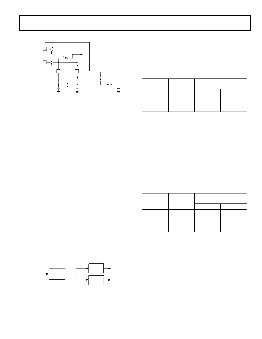
A third-overtone crystal can be used at frequencies above
25 MHz. The circuit is then modified to ensure crystal operation
only at the third overtone by adding a tuned inductor circuit as
shown in Figure 7. A design procedure for third-overtone oper-
ation is discussed in detail in an Application Note, Using Third
Overtone Crystals (EE-168).
The Blackfin core runs at a different clock rate than the on-chip
peripherals. As shown in Figure 8 on Page 19, the core clock
(CCLK) and system peripheral clock (SCLK) are derived from
the input clock (CLKIN) signal. An on-chip PLL is capable of
multiplying the CLKIN signal by a programmable 0.5
× to 64×
multiplication factor (bounded by specified minimum and max-
imum VCO frequencies). The default multiplier is 8
×, but it can
be modified by a software instruction sequence. This sequence
is managed by the bfrom_SysControl() function in the on-chip
ROM.
On-the-fly CCLK and SCLK frequency changes can be applied
by using the bfrom_SysControl() function in the on-chip ROM.
Whereas the maximum allowed CCLK and SCLK rates depend
on the applied voltages VDDINT and VDDEXT, the VCO is always
permitted to run up to the frequency specified by the part’s
speed grade.
The CLKOUT pin reflects the SCLK frequency to the off-chip
world. It functions as a reference for many timing specifications.
While inactive by default, it can be enabled using the
EBIU_AMGCTL register.
All on-chip peripherals are clocked by the system clock (SCLK).
The system clock frequency is programmable by means of the
SSEL3–0 bits of the PLL_DIV register. The values programmed
into the SSEL fields define a divide ratio between the PLL output
(VCO) and the system clock. SCLK divider values are 1 through
15. Table 7 illustrates typical system clock ratios. The default
ratio is 4.
Note that the divisor ratio must be chosen to limit the system
clock frequency to its maximum of fSCLK. The SSEL value can be
dynamically changed without any PLL lock latencies by writing
the appropriate values to the PLL divisor register (PLL_DIV)
using the bfrom_SysControl() function in the on-chip ROM.
The core clock (CCLK) frequency can also be dynamically
changed by means of the CSEL1–0 bits of the PLL_DIV register.
Supported CCLK divider ratios are 1, 2, 4, and 8, as shown in
Table 8. The default ratio is 1. This programmable core clock
capability is useful for fast core frequency modifications.
The maximum CCLK frequency not only depends on the part’s
speed grade, it also depends on the applied VDDINT voltage. See
Table 13 on Page 35 for details.
BOOTING MODES
The ADSP-BF54x Blackfin processors have many mechanisms
(listed in Table 9) for automatically loading internal and exter-
nal memory after a reset. The boot mode is specified by four
BMODE input pins dedicated to this purpose. There are two
categories of boot modes: master and slave. In master boot
Figure 7. External Crystal Connections
Note: For CCLK and SCLK specifications, see Table 16.
Figure 8. Frequency Modification Methods
CLKIN
CLKOUT
XTAL
EN
CLKBUF
TO PLL CIRCUITRY
F R OVERTONE
OPERA
O
TION ONLY
NOTE: VALUES MARKED WITH * MUST BE CUSTOMIZED
DEPENDING ON THE CRYSTAL AND LAYOUT. PLEASE
ANALYZE CAREFULLY.
18 pF*
EN
18 pF*
700
0
BLACKFIN
0
*
VDDEXT
1M
PLL
0.5x - 64x
1:15
1, 2, 4, 8
VCO
CLKIN
DYNAMIC MODIFICATION
REQUIRES PLL SEQUENCING
DYNAMIC MODIFICATION
ON-THE-FLY
CCLK
SCLK
Table 7. Example System Clock Ratios
Signal Name
SSEL3–0
Divider Ratio
VCO/SCLK
Example Frequency Ratios
(MHz)
VCO
SCLK
0010
2:1
200
100
0110
6:1
300
50
1010
10:1
500
50
Table 8. Core Clock Ratios
Signal Name
CSEL1–0
Divider Ratio
VCO/CCLK
Example Frequency Ratios
(MHz)
VCO
CCLK
00
1:1
300
01
2:1
300
150
10
4:1
500
125
11
8:1
200
25
相关PDF资料 |
PDF描述 |
|---|---|
| ADSP-21488KSWZ-4A | IC CCD SIGNAL PROCESSOR 100LQFP |
| ADSP-21488KSWZ-3A1 | IC DSP SHARC 400MHZ 100LQFP |
| JWS10028/A | PWR SUP 28.0V 3.6A SNG OUTPUT |
| MAX6505UTP020+T | IC TEMP SWITCH DL TRIP SOT23-6 |
| ADSP-BF533SBBZ400 | IC DSP CTLR 16BIT 400MHZ 169-BGA |
相关代理商/技术参数 |
参数描述 |
|---|---|
| AD5111 | 制造商:AD 制造商全称:Analog Devices 功能描述:Single-Channel, 128-/64-/32-Position, Up/Down, ±8% Resistor Tolerance, Nonvolatile Digital Potentiometer |
| AD5111BCPZ10-500R7 | 功能描述:IC DGTL POT 128POS 10K 8LFCSP RoHS:是 类别:集成电路 (IC) >> 数据采集 - 数字电位器 系列:- 标准包装:3,000 系列:DPP 接片:32 电阻(欧姆):10k 电路数:1 温度系数:标准值 300 ppm/°C 存储器类型:非易失 接口:3 线串行(芯片选择,递增,增/减) 电源电压:2.5 V ~ 6 V 工作温度:-40°C ~ 85°C 安装类型:表面贴装 封装/外壳:8-WFDFN 裸露焊盘 供应商设备封装:8-TDFN(2x3) 包装:带卷 (TR) |
| AD5111BCPZ10-RL7 | 功能描述:IC DGTL POT 128POS 10K 8LFCSP RoHS:是 类别:集成电路 (IC) >> 数据采集 - 数字电位器 系列:- 产品培训模块:Lead (SnPb) Finish for COTS Obsolescence Mitigation Program 标准包装:1 系列:- 接片:256 电阻(欧姆):100k 电路数:1 温度系数:标准值 35 ppm/°C 存储器类型:非易失 接口:3 线串口 电源电压:2.7 V ~ 5.25 V 工作温度:-40°C ~ 85°C 安装类型:表面贴装 封装/外壳:8-WDFN 裸露焊盘 供应商设备封装:8-TDFN-EP(3x3) 包装:剪切带 (CT) 产品目录页面:1399 (CN2011-ZH PDF) 其它名称:MAX5423ETA+TCT |
| AD5111BCPZ80-500R7 | 功能描述:IC DGTL POT 128POS 80K 8LFCSP RoHS:是 类别:集成电路 (IC) >> 数据采集 - 数字电位器 系列:- 标准包装:3,000 系列:DPP 接片:32 电阻(欧姆):10k 电路数:1 温度系数:标准值 300 ppm/°C 存储器类型:非易失 接口:3 线串行(芯片选择,递增,增/减) 电源电压:2.5 V ~ 6 V 工作温度:-40°C ~ 85°C 安装类型:表面贴装 封装/外壳:8-WFDFN 裸露焊盘 供应商设备封装:8-TDFN(2x3) 包装:带卷 (TR) |
| AD5111BCPZ80-RL7 | 功能描述:IC DGTL POT 128POS 80K 8LFCSP RoHS:是 类别:集成电路 (IC) >> 数据采集 - 数字电位器 系列:- 产品培训模块:Lead (SnPb) Finish for COTS Obsolescence Mitigation Program 标准包装:1 系列:- 接片:256 电阻(欧姆):100k 电路数:1 温度系数:标准值 35 ppm/°C 存储器类型:非易失 接口:3 线串口 电源电压:2.7 V ~ 5.25 V 工作温度:-40°C ~ 85°C 安装类型:表面贴装 封装/外壳:8-WDFN 裸露焊盘 供应商设备封装:8-TDFN-EP(3x3) 包装:剪切带 (CT) 产品目录页面:1399 (CN2011-ZH PDF) 其它名称:MAX5423ETA+TCT |
发布紧急采购,3分钟左右您将得到回复。