- 您现在的位置:买卖IC网 > PDF目录3987 > IDT70V657S12BF8 (IDT, Integrated Device Technology Inc)IC SRAM 1.125MBIT 12NS 208FBGA PDF资料下载
参数资料
| 型号: | IDT70V657S12BF8 |
| 厂商: | IDT, Integrated Device Technology Inc |
| 文件页数: | 13/24页 |
| 文件大小: | 0K |
| 描述: | IC SRAM 1.125MBIT 12NS 208FBGA |
| 标准包装: | 1,000 |
| 格式 - 存储器: | RAM |
| 存储器类型: | SRAM - 双端口,异步 |
| 存储容量: | 1.125M(32K x 36) |
| 速度: | 12ns |
| 接口: | 并联 |
| 电源电压: | 3.15 V ~ 3.45 V |
| 工作温度: | 0°C ~ 70°C |
| 封装/外壳: | 208-LFBGA |
| 供应商设备封装: | 208-CABGA(15x15) |
| 包装: | 带卷 (TR) |
| 其它名称: | 70V657S12BF8 |
�� �
�
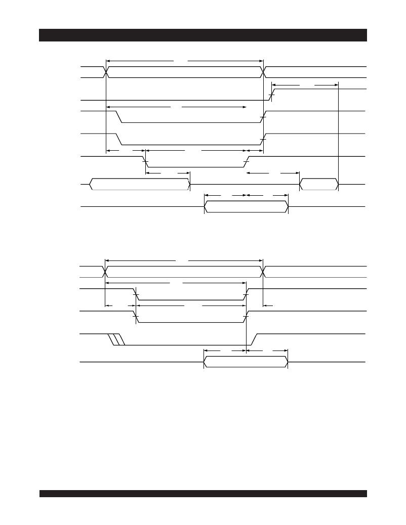
�IDT70V659/58/57S�
�High-Speed� 3.3V� 128/64/32K� x� 36� Asynchronous� Dual-Port� Static� RAM�
�Industrial� and� Commercial� Temperature� Ranges�
�Timing� Waveform� of� Write� Cycle� No.� 1,� R/� W� Controlled� Timing� (1,5,8)�
�t� WC�
�ADDRESS�
�OE�
�t� AW�
�t� HZ�
�(7)�
�CE� or� SEM�
�(9)�
�BE� n�
�(9)�
�t� AS� (6)�
�t� WP�
�(2)�
�t� WR�
�(3)�
�R/� W�
�t� WZ� (7)�
�t� OW�
�DATA� OUT�
�(4)�
�t� DW�
�t� DH�
�(4)�
�DATA� IN�
�4869� drw� 08�
�Timing� Waveform� of� Write� Cycle� No.� 2,� CE� Controlled� Timing� (1,5)�
�t� WC�
�ADDRESS�
�t� AW�
�CE� or� SEM�
�(9)�
�t� AS�
�BE� n�
�(9)�
�R/� W�
�DATA� IN�
�(6)�
�t� EW� (2)�
�t� DW�
�t� WR� (3)�
�t� DH�
�4869� drw� 09�
�.�
�NOTES:�
�1.� R/� W� or� CE� or� BE� n� =� V� IH� during� all� address� transitions.�
�2.� A� write� occurs� during� the� overlap� (t� EW� or� t� WP� )� of� a� CE� =� V� IL� and� a� R/� W� =� V� IL� for� memory� array� writing� cycle.�
�3.� t� WR� is� measured� from� the� earlier� of� CE� or� R/� W� (or� SEM� or� R/� W� )� going� HIGH� to� the� end� of� write� cycle.�
�4.� During� this� period,� the� I/O� pins� are� in� the� output� state� and� input� signals� must� not� be� applied.�
�5.� If� the� CE� or� SEM� =� V� IL� transition� occurs� simultaneously� with� or� after� the� R/� W� =� V� IL� transition,� the� outputs� remain� in� the� High-impedance� state.�
�6.� Timing� depends� on� which� enable� signal� is� asserted� last,� CE� or� R/� W� .�
�7.� This� parameter� is� guaranteed� by� device� characterization,� but� is� not� production� tested.� Transition� is� measured� 0mV� from� steady� state� with� the� Output� Test� Load�
�(Figure� 2).�
�8.� If� OE� =� V� IL� during� R/W� controlled� write� cycle,� the� write� pulse� width� must� be� the� larger� of� t� WP� or� (t� WZ� +� t� DW� )� to� allow� the� I/O� drivers� to� turn� off� and� data� to� be�
�placed� on� the� bus� for� the� required� t� DW� .� If� OE� =� V� IH� during� an� R/� W� controlled� write� cycle,� this� requirement� does� not� apply� and� the� write� pulse� can� be� as� short� as� the�
�specified� t� WP� .�
�9.� To� access� RAM,� CE� =� V� IL� and� SEM� =� V� IH� .� To� access� semaphore,� CE� =� V� IH� and� SEM� =� V� IL� .� t� EW� must� be� met� for� either� condition.�
�13�
�相关PDF资料 |
PDF描述 |
|---|---|
| KMPC8560PX833LC | IC MPU POWERQUICC III 783-FCPBGA |
| KMPC8560PX833LB | IC MPU POWERQUICC III 783-FCPBGA |
| IDT70V657S12BC8 | IC SRAM 1.125MBIT 12NS 256BGA |
| KMPC8560PX667LB | IC MPU POWERQUICC III 783-FCPBGA |
| IDT70V3389S6PRF8 | IC SRAM 1.125MBIT 6NS 128TQFP |
相关代理商/技术参数 |
参数描述 |
|---|---|
| AD622ARZ-RL7 | 制造商:AD 制造商全称:Analog Devices 功能描述:Low Cost Instrumentation Amplifier |
| AD623 | 制造商:AD 制造商全称:Analog Devices 功能描述:Single Supply, Rail-to-Rail, Low Cost Instrumentation Amplifier |
| AD623-00E | 功能描述:SENSOR MAG SW 80G CROS AX 8-MSOP 制造商:nve corp/sensor products 系列:AD 包装:管件 零件状态:有效 功能:全极开关 技术:霍尔效应 极化:任意一种 感应范围:±10mT 跳闸,±6.5mT 释放 测试条件:-40°C ~ 125°C 电压 - 电源:4.5 V ~ 30 V 电流 - 电源(最大值):4.5mA 电流 - 输出(最大值):20mA 输出类型:开路集电极 特性:- 工作温度:-40°C ~ 125°C(TA) 封装/外壳:8-TSSOP,8-MSOP(0.118",3.00mm 宽) 供应商器件封装:8-MSOP 标准包装:1,000 |
| AD623-02E | 功能描述:SENSOR MAG SW 80G CROS AXS 8SOIC 制造商:nve corp/sensor products 系列:AD 包装:管件 零件状态:有效 功能:全极开关 技术:霍尔效应 极化:任意一种 感应范围:±10mT 跳闸,±6.5mT 释放 测试条件:-40°C ~ 125°C 电压 - 电源:4.5 V ~ 30 V 电流 - 电源(最大值):4.5mA 电流 - 输出(最大值):20mA 输出类型:开路集电极 特性:- 工作温度:-40°C ~ 125°C(TA) 封装/外壳:8-SOIC(0.154",3.90mm 宽) 供应商器件封装:8-SOIC 标准包装:1,000 |
| AD6231 | 制造商:AD 制造商全称:Analog Devices 功能描述:10 MHz, 20 V/レs, G = 1, 10, 100, 1000 i CMOS㈢ Programmable Gain Instrumentation Amplifier |
发布紧急采购,3分钟左右您将得到回复。