- 您现在的位置:买卖IC网 > PDF目录11657 > AD694BRZ-REEL (Analog Devices Inc)IC TRANSMITTER 4-20MA 16-SOIC PDF资料下载
参数资料
| 型号: | AD694BRZ-REEL |
| 厂商: | Analog Devices Inc |
| 文件页数: | 16/16页 |
| 文件大小: | 0K |
| 描述: | IC TRANSMITTER 4-20MA 16-SOIC |
| 标准包装: | 1,000 |
| 类型: | 电流发送器 |
| 输入类型: | 电压 |
| 输出类型: | 电压 |
| 电流 - 电源: | 23mA |
| 安装类型: | 表面贴装 |
| 封装/外壳: | 16-SOIC(0.295",7.50mm 宽) |
| 供应商设备封装: | 16-SOIC W |
| 包装: | 带卷 (TR) |
AD694
REV. B
–9–
Figure 8. Span Adjustment, 2 V Full Scale
PROGRAMMING OTHER SPANS
There are two methods for programming input spans less than
10 V. The first decreases the input span by programming a non-
inverting gain into the buffer amplifier. For example, to achieve
an input span of 0–5 V, the AD694 is set in its 10 V full-scale
mode and the buffer amplifier is configured with a noninverting
gain of 2 by adding 2 resistors. Now a 5 V signal at +Sig results
in a 10 V full-scale signal at FB (Pin 1), the input to the V/I.
This method requires that the V/I be programmed to a 10 V full
scale for input spans between 2 V to 10 V. It should be pro-
grammed to a 2 V full scale if input spans of less than 2 V are
required. This adjustment scheme makes the accuracy of the
span adjustment dependent upon the ratio accuracy of the re-
quired gain resistors. Thus, it is possible to accurately configure
spans other than 2 V or 10 V without using trimming potenti-
ometers, given that the resistor ratios are sufficiently accurate. A
supply voltage of 12.5 V is required for spans between 2 V and
10 V. Spans below 2 V require a VS of 4.5 V or greater.
A second method, allows other spans of less than 10 V to be
programmed when supply voltage is less than 12.5 V. Since the
AD694 amplifiers require 2.5 V of headroom for operation, a
5 V full-scale input is possible with a 7.5 V supply. This is
achieved by placing a resistor, in parallel with R2, (2 V FS [Pin
4] to Com [Pin 5]), to adjust the transconductance of the V/I
converter without a headroom penalty. A disadvantage of this
method is that the external resistor must match the internal re-
sistor in a precise manner, thus a span trim will be required.
The value should be chosen to allow for the
±10% uncertainty
in the absolute value of the internal resistor R2.
ADJUSTING REFERENCE OUTPUT
Figure 9 shows one method of making small adjustments to the
10 V reference output. This circuit allows a linear adjustment
range of
±200 mV. The 2 V reference may also be adjusted but
only in the positive direction.
Other reference voltages can be programmed by adding external
resistors. For example, a resistor placed in parallel with R5 can
be added to boost the reference output as high as 20 V. Con-
versely, a resistor in parallel with R6 can be used to set the refer-
ence voltage to a value between 2 V and 10 V. The output
voltage VREF = 2 V (R6 + R5)/R5. In choosing external
adjustment resistors remember that the internal resistors, while
ratio matched to a high degree of accuracy, have an absolute re-
sistor tolerance of only
±10%. Be prepared to compensate for
this if a precise voltage other than the precalibrated values of 2
V or 10 V is required.
Figure 9. 10 V Reference Output Adjustment
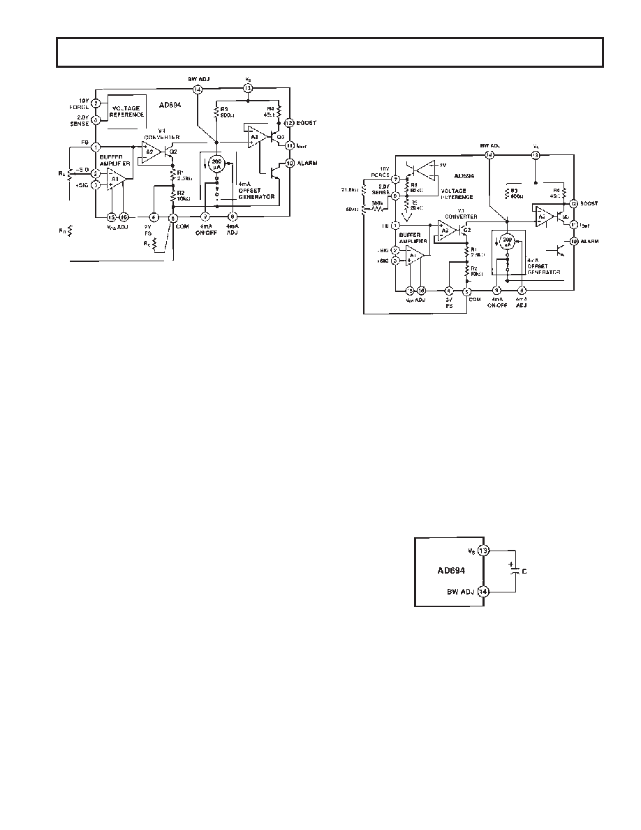
BANDWIDTH CONTROL
The bandwidth of the AD694 can be limited to provide noise
filtering. This is achieved by connecting an external capacitor
from BW ADJ (Pin 14) to VS (Pin 13) as shown in Figure 10.
To program the bandwidth, substitute the desired bandwidth in
Hz, into the formula below to determine the required capacitor.
C
BW
=×
×
12
900
/(
)
π
The bandwidth chosen will vary
±10% due to internal resistor
tolerance, plus an additional amount due to capacitor tolerance.
This method of bandwidth control is not recommended as a
way to filter large high frequency transients in the input signal.
It is recommended that frequencies greater than the BW of the
buffer amplifier be eliminated with an input filter to avoid recti-
fication of noise by the input amplifiers.
Figure 10. Noise Filtering with an External Capacitor
BUFFER AMPLIFIER OFFSET ADJUST
The buffer amplifier input voltage offset has been laser trimmed
to a high degree of accuracy; however, there may be occasions
when an offset trim is desired. Figure 11 shows the adjustment
method; a trim range of greater than
±2.5 mV is available with
this scheme. It is not recommended that this adjustment
method be used to affect the 4 mA offset current as the trim will
induce offset drift into the buffer amplifier. The buffer amplifier
will drift approximately 1
V/°C for each 300 V of induced
offset. To adjust the 4 mA offset current refer to the Adjusting
4 mA Zero section.
相关PDF资料 |
PDF描述 |
|---|---|
| VE-JNH-IY-F1 | CONVERTER MOD DC/DC 52V 50W |
| VI-JTK-IW-F2 | CONVERTER MOD DC/DC 40V 100W |
| VE-JNP-IY-F2 | CONVERTER MOD DC/DC 13.8V 50W |
| VI-JTJ-IW-F1 | CONVERTER MOD DC/DC 36V 100W |
| VI-JTH-IW-F3 | CONVERTER MOD DC/DC 52V 100W |
相关代理商/技术参数 |
参数描述 |
|---|---|
| AD694BRZ-REEL7 | 功能描述:IC TRANSMITTER 4-20MA 16-SOIC RoHS:是 类别:集成电路 (IC) >> 接口 - 传感器和探测器接口 系列:- 其它有关文件:Automotive Product Guide 产品培训模块:Lead (SnPb) Finish for COTS Obsolescence Mitigation Program 标准包装:74 系列:- 类型:触控式传感器 输入类型:数字 输出类型:数字 接口:JTAG,串行 电流 - 电源:100µA 安装类型:表面贴装 封装/外壳:20-TSSOP(0.173",4.40mm 宽) 供应商设备封装:20-TSSOP 包装:管件 |
| AD694JN | 制造商:Analog Devices 功能描述:SP Amp INSTR Amp Single 36V 16-Pin PDIP Tube 制造商:Analog Devices 功能描述:TRANSMITTER 420MA SMD DIP16 694 |
| AD694JN | 制造商:Analog Devices 功能描述:SEMICONDUCTORSLINEAR |
| AD694JNZ | 功能描述:IC TRANSMITTER 4-20MA 16-DIP RoHS:是 类别:集成电路 (IC) >> 接口 - 传感器和探测器接口 系列:- 其它有关文件:Automotive Product Guide 产品培训模块:Lead (SnPb) Finish for COTS Obsolescence Mitigation Program 标准包装:74 系列:- 类型:触控式传感器 输入类型:数字 输出类型:数字 接口:JTAG,串行 电流 - 电源:100µA 安装类型:表面贴装 封装/外壳:20-TSSOP(0.173",4.40mm 宽) 供应商设备封装:20-TSSOP 包装:管件 |
| AD694JR | 功能描述:IC TRANSMITTER 4-20MA 制造商:analog devices inc. 系列:- 包装:散装 零件状态:上次购买时间 类型:电流发送器 输入类型:电压 输出类型:电压 接口:- 电流 - 电源:23mA 工作温度:0°C ~ 70°C 安装类型:表面贴装 封装/外壳:16-SOIC(0.154",3.90mm 宽) 供应商器件封装:16-SOIC 标准包装:1 |
发布紧急采购,3分钟左右您将得到回复。