- 您现在的位置:买卖IC网 > PDF目录373901 > AD7477SRT-REEL7 (ANALOG DEVICES INC) 1 MSPS, 12-/10-/8-Bit ADCs in 6-Lead SOT-23 PDF资料下载
参数资料
| 型号: | AD7477SRT-REEL7 |
| 厂商: | ANALOG DEVICES INC |
| 元件分类: | ADC |
| 英文描述: | 1 MSPS, 12-/10-/8-Bit ADCs in 6-Lead SOT-23 |
| 中文描述: | 1-CH 10-BIT SUCCESSIVE APPROXIMATION ADC, SERIAL ACCESS, PDSO6 |
| 封装: | PLASTIC, MO-178AB, SOT-23, 6 PIN |
| 文件页数: | 13/20页 |
| 文件大小: | 360K |
| 代理商: | AD7477SRT-REEL7 |
REV. D
AD7476/AD7477/AD7478
–13–
conversion result.
CS
may idle high until the next conversion or
may idle low until
CS
returns high sometime prior to the next
conversion (effectively idling
CS
low).
Once a data transfer is complete (SDATA has returned to three-
state), another conversion can be initiated after the quiet time,
t
QUIET
, has elapsed by again bringing
CS
low.
Power-Down Mode
This mode is intended for use in applications where slower
throughput rates are required; either the ADC is powered down
between each conversion, or a series of conversions may be
performed at a high throughput rate and the ADC is then powered
down for a relatively long duration between these bursts of several
conversions. When the AD7476/AD7477/AD7478 is in power-
down, all analog circuitry is powered down.
To enter power-down, the conversion process must be interrupted
by bringing
CS
high any time after the second falling edge of
SCLK and before the tenth falling edge of SCLK, as shown in
Figure 12. Once
CS
has been brought high in this window of
SCLKs, the part will enter power-down and the conversion that
was initiated by the falling edge of
CS
will be terminated and
SDATA will go back into three-state. If
CS
is brought high before
the second SCLK falling edge, the part will remain in Normal mode
and will not power down. This will avoid accidental power-down
due to glitches on the
CS
line.
To exit this mode of operation and power up the AD7476/
AD7477/AD7478 again, a dummy conversion is performed. On
the falling edge of
CS
, the device will begin to power up, and
will continue to power up as long as
CS
is held low until after the
falling edge of the tenth SCLK. The device will be fully powered
up once 16 SCLKs have elapsed and, as shown in Figure 13,
valid data will result from the next conversion. If
CS
is brought
high before the tenth falling edge of SCLK, the AD7476/
AD7477/AD7478 will again go back into power-down. This
avoids accidental power-up due to glitches on the
CS
line or an
inadvertent burst of eight SCLK cycles while
CS
is low. So
although the device may begin to power up on the falling edge
of
CS
, it will again power down on the rising edge of
CS
as long
as it occurs before the tenth SCLK falling edge.
Power-Up Time
The power-up time of the AD7476/AD7477/AD7478 is typically
1 s, which means that with any frequency of SCLK up to
20 MHz, one dummy cycle will always be sufficient to allow the
device to power up. Once the dummy cycle is complete, the ADC
will be fully powered up and the input signal will be acquired
properly. The quiet time (t
QUIET
) must still be allowed from the
point at which the bus goes back into three-state after the dummy
conversion, to the next falling edge of
CS
. When running at
1 MSPS throughput rate, the AD7476/AD7477/AD7478 will
power up and acquire a signal within
±
0.5 LSB in one dummy
cycle, i.e., 1 s.
When powering up from the Power-Down mode with a dummy
cycle, as in Figure 13, the track-and-hold that was in Hold
mode while the part was powered down returns to Track mode
after the first SCLK edge the part receives after the falling edge of
CS
. This is shown as Point A in Figure 13. Although at any
SCLK frequency one dummy cycle is sufficient to power up the
device and acquire V
IN
, it does not necessarily mean that a full
dummy cycle of 16 SCLKs must always elapse to power up the
device and fully acquire V
IN
; 1
μ
s will be sufficient to power up the
device and acquire the input signal. If, for example, a 5 MHz
SCLK frequency were applied to the ADC, the cycle time would
be 3.2
μ
s. In one dummy cycle, 3.2
μ
s, the part would be powered
up and V
IN
fully acquired. However, after 1
μ
s with a 5 MHz
SCLK, only five SCLK cycles would have elapsed. At this stage,
the ADC would be fully powered up and the signal acquired. So,
in this case, the
CS
can be brought high after the tenth SCLK
falling edge and brought low again after a time t
QUIET
to initiate
the conversion.
When power supplies are first applied to the AD7476/AD7477/
AD7478, the ADC may power up in either Power-Down mode
or Normal mode. Because of this, it is best to allow a dummy
cycle to elapse to ensure the part is fully powered up before
attempting a valid conversion. Likewise, if it is intended to keep
the part in the Power-Down mode while not in use and the user
wants the part to power up in Power-Down mode, the dummy
cycle may be used to ensure the device is in power-down by
executing a cycle such as that shown in Figure 12. Once supplies
are applied to the AD7476/AD7477/AD7478, the power-up
time is the same as that when powering up from the Power-Down
mode. It takes approximately 1
μ
s to fully power up if the part
powers up in Normal mode. It is not necessary to wait 1
μ
s before
executing a dummy cycle to ensure the desired mode of operation.
Instead, the dummy cycle can occur directly after power is supplied
to the ADC. If the first valid conversion is then performed directly
after the dummy conversion, care must be taken to ensure that
adequate acquisition time has been allowed. As mentioned earlier,
when powering up from the Power-Down mode, the part will
return to track upon the first SCLK edge applied after the falling
edge of
CS
. However, when the ADC powers up initially after
supplies are applied, the track-and-hold will already be in track.
This means that if the ADC powers up in the desired mode of
operation, and a dummy cycle is not required to change mode, then
a dummy cycle is not required to place the track-and-hold
into track.
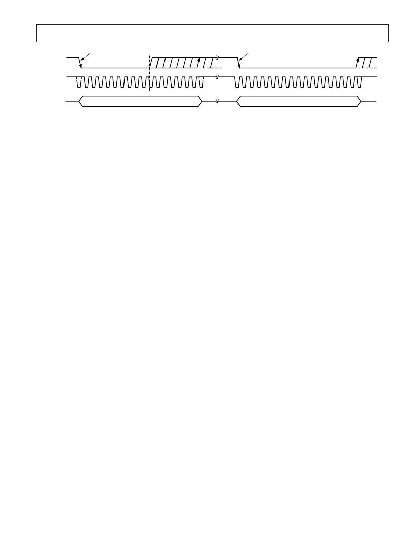
1
10
16
16
1
A
CS
SCLK
SDATA
THE PART BEGINS
TO POWER UP
THE PART IS FULLY POWERED
UP WITH V
IN
FULLY ACQUIRED
INVALID DATA
VALID DATA
Figure 13. Exiting Power-Down Mode
相关PDF资料 |
PDF描述 |
|---|---|
| AD7476ARTZ-REEL | LED Indicator; LED Color:Amber; Color:Amber; Lens Color:Amber; Lens Style:Flush; Body Material:Metal RoHS Compliant: Yes |
| AD7476BRTZ-REEL | 1 MSPS, 12-/10-/8-Bit ADCs in 6-Lead SOT-23 |
| AD7476ART | 1 MSPS, 12-/10-/8-Bit ADCs in 6-Lead SOT-23 |
| AD7476BRT | +3.3V, 2.125Gbps/1.0625Gbps Fibre-Channel Port Bypass ICs |
| AD7476BRT-REEL | +3.3V, 2.125Gbps/1.0625Gbps Fibre-Channel Port Bypass ICs |
相关代理商/技术参数 |
参数描述 |
|---|---|
| AD7477SRTZ-REEL | 功能描述:模数转换器 - ADC 10Bit 1MSPS Lo-Pwr RoHS:否 制造商:Analog Devices 通道数量: 结构: 转换速率: 分辨率: 输入类型: 信噪比: 接口类型: 工作电源电压: 最大工作温度: 安装风格: 封装 / 箱体: |
| AD7477SRTZ-REEL3 | 制造商:AD 制造商全称:Analog Devices 功能描述:1 MSPS, 12-/10-/8-Bit ADCs in 6-Lead SOT-23 |
| AD7477SRTZ-REEL7 | 制造商:Analog Devices 功能描述:ADC Single SAR 1Msps 10-bit Serial 6-Pin SOT-23 T/R |
| AD7478 | 制造商:AD 制造商全称:Analog Devices 功能描述:1 MSPS, 12-/10-/8-Bit ADCs in 6-Lead SOT-23 |
| AD7478A | 制造商:未知厂家 制造商全称:未知厂家 功能描述:AD7476A/AD7477A/AD7478A: 2.35 V to 5.25 V. 1 MSPS. 12-/10-/8-Bit ADCs in 6-Lead SC70 Data Sheet (Rev. A. 2/03) |
发布紧急采购,3分钟左右您将得到回复。