- 您现在的位置:买卖IC网 > PDF目录373901 > AD7477SRT-REEL7 (ANALOG DEVICES INC) 1 MSPS, 12-/10-/8-Bit ADCs in 6-Lead SOT-23 PDF资料下载
参数资料
| 型号: | AD7477SRT-REEL7 |
| 厂商: | ANALOG DEVICES INC |
| 元件分类: | ADC |
| 英文描述: | 1 MSPS, 12-/10-/8-Bit ADCs in 6-Lead SOT-23 |
| 中文描述: | 1-CH 10-BIT SUCCESSIVE APPROXIMATION ADC, SERIAL ACCESS, PDSO6 |
| 封装: | PLASTIC, MO-178AB, SOT-23, 6 PIN |
| 文件页数: | 14/20页 |
| 文件大小: | 360K |
| 代理商: | AD7477SRT-REEL7 |
REV. D
–14–
AD7476/AD7477/AD7478
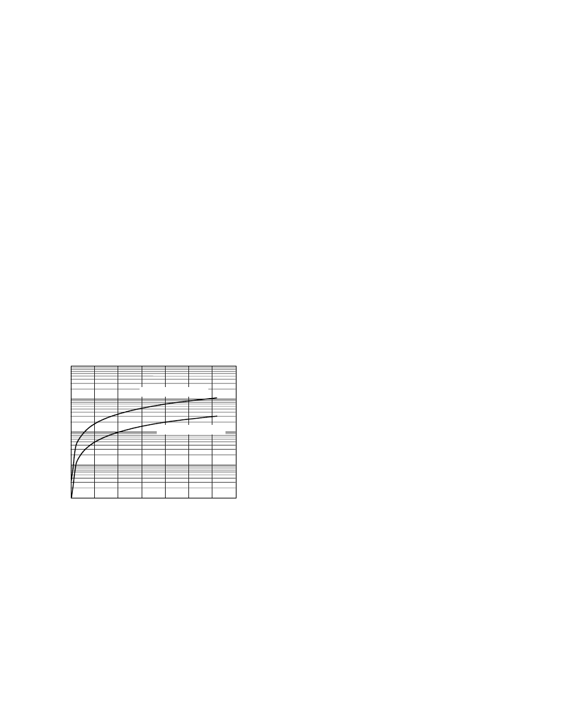
POWER VS. THROUGHPUT RATE
By using the Power-Down mode on the AD7476/AD7477/AD7478
when not converting, the average power consumption of the ADC
decreases at lower throughput rates. Figure 14 shows how as the
throughput rate is reduced, the device remains in its power-down
state longer, and the average power consumption over time
drops accordingly.
For example, if the AD7476/AD7477/AD7478 is operated in a
continuous sampling mode with a throughput rate of 100 kSPS
and a SCLK of 20 MHz (V
DD
= 5 V), and the device is placed
in the Power-Down mode between conversions, then the power
consumption is calculated as follows. The power dissipation
during normal operation is 17.5 mW (V
DD
= 5 V). If the
power-up time is one dummy cycle, i.e., 1
μ
s, and the remaining
conversion time is another cycle, i.e., 1
μ
s, then the AD7476/
AD7477/AD7478 can be said to dissipate 17.5 mW for 2
μ
s
during each conversion cycle. If the throughput rate is 100 kSPS,
the cycle time is 10
μ
s and the average power dissipated
during each cycle is (2/10)
×
(17.5 mW) = 3.5 mW. If V
DD
=
3 V, SCLK = 20 MHz, and the device is again in Power-Down
mode between conversions, the power dissipation during normal
operation is 4.8 mW. The AD7476/AD7477/AD7478 can now
be said to dissipate 4.8 mW for 2
μ
s during each conversion
cycle. With a throughput rate of 100 kSPS, the average power
dissipated during each cycle is (2/10)
×
(4.8 mW) = 0.96 mW.
Figure 14 shows the power versus throughput rate when using
the Power-Down mode between conversions with both 5 V
and 3 V supplies.
THROUGHPUT RATE – kSPS
100
0
P
10
1
0.1
0.01
50
100
150
200
250
300
350
V
DD
= 5V, SCLK = 20MHz
V
DD
= 3V, SCLK = 20MHz
Figure 14. Power vs. Throughput Rate
The Power-Down mode is intended for use with throughput
rates of approximately 333 kSPS and under, because at higher
sampling rates power is not saved by using the Power-Down mode.
SERIAL INTERFACE
Figures 15, 16, and 17 show the detailed timing diagrams for
serial interfacing to the AD7476, AD7477, and AD7478,
respectively. The serial clock provides the conversion clock
and also controls the transfer of information from the AD7476/
AD7477/AD7478 during conversion.
The
CS
signal initiates the data transfer and conversion process.
The falling edge of
CS
puts the track-and-hold into Hold mode,
takes the bus out of three-state, and the analog input is sampled
at this point. The conversion is also initiated at this point and
will require sixteenth SCLK cycles to complete. Once 13 SCLK
falling edges have elapsed, the track-and-hold will go back into
track on the next SCLK rising edge as shown in Figures 15, 16,
and 17 at Point B. On the sixteenth SCLK falling edge, the
SDATA line will go back into three-state. If the rising edge of
CS
occurs before 16 SCLKs have elapsed, the conversion will be
terminated and the SDATA line will go back into three-state;
otherwise, SDATA returns to three-state on the sixteenth SCLK
falling edge as shown in Figures 15, 16, and 17. Sixteen serial
clock cycles are required to perform the conversion process
and to access data from the AD7476/AD7477/AD7478.
CS
going low provides the first leading zero to be read in by the
microcontroller or DSP. The remaining data is then clocked out
by subsequent SCLK falling edges, beginning with the second
leading zero. Thus the first falling clock edge on the serial clock
has the first leading zero provided and also clocks out the second
leading zero. The final bit in the data transfer is valid on the
sixteenth falling edge, having been clocked out on the previous
(fifteenth) falling edge. In applications with a slower SCLK, it
is possible to read in data on each SCLK rising edge, i.e., al-
though the first leading zero will have to be read on the first
SCLK falling edge after the
CS
falling edge. Therefore, the first
rising edge of SCLK after the
CS
falling edge will provide the
second leading zero and the fifteenth rising SCLK edge will have
DB0 provided or the final zero for the AD7477 and AD7478.
This may not work with most microcontrollers/DSPs, but could
possibly be used with FPGAs and ASICs.
相关PDF资料 |
PDF描述 |
|---|---|
| AD7476ARTZ-REEL | LED Indicator; LED Color:Amber; Color:Amber; Lens Color:Amber; Lens Style:Flush; Body Material:Metal RoHS Compliant: Yes |
| AD7476BRTZ-REEL | 1 MSPS, 12-/10-/8-Bit ADCs in 6-Lead SOT-23 |
| AD7476ART | 1 MSPS, 12-/10-/8-Bit ADCs in 6-Lead SOT-23 |
| AD7476BRT | +3.3V, 2.125Gbps/1.0625Gbps Fibre-Channel Port Bypass ICs |
| AD7476BRT-REEL | +3.3V, 2.125Gbps/1.0625Gbps Fibre-Channel Port Bypass ICs |
相关代理商/技术参数 |
参数描述 |
|---|---|
| AD7477SRTZ-REEL | 功能描述:模数转换器 - ADC 10Bit 1MSPS Lo-Pwr RoHS:否 制造商:Analog Devices 通道数量: 结构: 转换速率: 分辨率: 输入类型: 信噪比: 接口类型: 工作电源电压: 最大工作温度: 安装风格: 封装 / 箱体: |
| AD7477SRTZ-REEL3 | 制造商:AD 制造商全称:Analog Devices 功能描述:1 MSPS, 12-/10-/8-Bit ADCs in 6-Lead SOT-23 |
| AD7477SRTZ-REEL7 | 制造商:Analog Devices 功能描述:ADC Single SAR 1Msps 10-bit Serial 6-Pin SOT-23 T/R |
| AD7478 | 制造商:AD 制造商全称:Analog Devices 功能描述:1 MSPS, 12-/10-/8-Bit ADCs in 6-Lead SOT-23 |
| AD7478A | 制造商:未知厂家 制造商全称:未知厂家 功能描述:AD7476A/AD7477A/AD7478A: 2.35 V to 5.25 V. 1 MSPS. 12-/10-/8-Bit ADCs in 6-Lead SC70 Data Sheet (Rev. A. 2/03) |
发布紧急采购,3分钟左右您将得到回复。