- 您现在的位置:买卖IC网 > PDF目录19717 > TOP261LG (Power Integrations)IC OFFLINE SWIT PROG OVP 7FESIP PDF资料下载
参数资料
| 型号: | TOP261LG |
| 厂商: | Power Integrations |
| 文件页数: | 22/50页 |
| 文件大小: | 0K |
| 描述: | IC OFFLINE SWIT PROG OVP 7FESIP |
| 标准包装: | 48 |
| 系列: | TOPSwitch®-HX |
| 输出隔离: | 隔离 |
| 频率范围: | 119kHz ~ 145kHz |
| 输出电压: | 700V |
| 功率(瓦特): | 244W |
| 工作温度: | -40°C ~ 150°C |
| 封装/外壳: | 7-SIP,6 引线,裸露焊盘,成形引线 |
| 供应商设备封装: | eSIP-7F |
| 包装: | 管件 |
第1页第2页第3页第4页第5页第6页第7页第8页第9页第10页第11页第12页第13页第14页第15页第16页第17页第18页第19页第20页第21页当前第22页第23页第24页第25页第26页第27页第28页第29页第30页第31页第32页第33页第34页第35页第36页第37页第38页第39页第40页第41页第42页第43页第44页第45页第46页第47页第48页第49页第50页
�� �
�
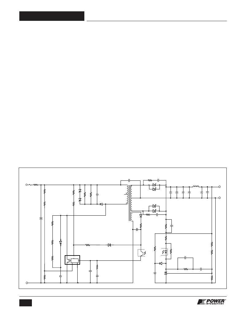
�TOP252-262�
�A� High� Efficiency,� 150� W,� 250� –� 380� VDC� Input�
�Power� Supply�
�The� circuit� shown� in� Figure� 42� delivers� 150� W� (19� V� @� 7.7� A)� at�
�84%� efficiency� using� a� TOP258Y� from� a� 250� VDC� to� 380� VDC�
�input.� A� DC� input� is� shown,� as� typically� at� this� power� level� a�
�power� factor� correction� stage� would� precede� this� supply,�
�providing� the� DC� input.� Capacitor� C1� provides� local� decoupling,�
�necessary� when� the� supply� is� remote� from� the� main� PFC� output�
�capacitor.�
�The� flyback� topology� is� still� usable� at� this� power� level� due� to� the�
�high� output� voltage,� keeping� the� secondary� peak� currents� low�
�enough� so� that� the� output� diode� and� capacitors� are� reasonably�
�sized.� In� this� example,� the� TOP258YN� is� at� the� upper� limit� of� its�
�dissipated� by� VR1� and� VR3,� the� leakage� energy� instead� being�
�dissipated� by� R1� and� R2.� However,� VR1� and� VR3� are� essential�
�to� limit� the� peak� drain� voltage� during� start-up� and/or� overload�
�conditions� to� below� the� 700� V� rating� of� the� TOPSwitch-HX�
�MOSFET.� The� schematic� shows� an� additional� turn-off� snubber�
�circuit� consisting� of� R20,� R21,� R22,� D5� and� C18.� This� reduces�
�turn-off� losses� in� the� TOPSwitch-HX.�
�The� secondary� is� rectified� and� smoothed� by� D2,� D3� and� C5,�
�C6,� C7� and� C8.� Two� windings� are� used� and� rectified� with�
�separate� diodes� D2� and� D3� to� limit� diode� dissipation.� Four�
�capacitors� are� used� to� ensure� their� maximum� ripple� current�
�specification� is� not� exceeded.� Inductor� L1� and� capacitors� C15�
�and� C16� provide� switching� noise� filtering.�
�power� capability.�
�Output� voltage� is� controlled� using� a� TL431� reference� IC� and�
�Resistors� R3,� R6� and� R7� provide� output� power� limiting,�
�maintaining� relatively� constant� overload� power� with� input� voltage.�
�Line� sensing� is� implemented� by� connecting� a� 4� M� W� resistor� from�
�the� V� pin� to� the� DC� rail.� Resistors� R4� and� R5� together� form� the�
�4� M� W� line� sense� resistor.� If� the� DC� input� rail� rises� above�
�450� VDC,� then� TOPSwitch-HX� will� stop� switching� until� the�
�voltage� returns� to� normal,� preventing� device� damage.�
�Due� to� the� high� primary� current,� a� low� leakage� inductance�
�transformer� is� essential.� Therefore,� a� sandwich� winding� with� a�
�copper� foil� secondary� was� used.� Even� with� this� technique,� the�
�leakage� inductance� energy� is� beyond� the� power� capability� of� a�
�simple� Zener� clamp.� Therefore,� R1,� R2� and� C3� are� added� in�
�parallel� to� VR1� and� VR3,� two� series� TVS� diodes� being� used� to�
�reduce� dissipation.� During� normal� operation,� very� little� power� is�
�R15,� R16� and� R17� to� form� a� potential� divider� to� sense� the�
�output� voltage.� Resistor� R12� and� R24� together� limit� the�
�optocoupler� LED� current� and� set� overall� control� loop� DC� gain.�
�Control� loop� compensation� is� achieved� using� components� C12,�
�C13,� C20� and� R13.� Diode� D6,� resistor� R23� and� capacitor� C19�
�form� a� soft� finish� network.� This� feeds� current� into� the� control�
�pin� prior� to� output� regulation,� preventing� output� voltage�
�overshoot� and� ensuring� startup� under� low� line,� full� load�
�conditions.�
�Sufficient� heat� sinking� is� required� to� keep� the� TOPSwitch-HX�
�device� below� 110� °� C� when� operating� under� full� load,� low� line�
�and� maximum� ambient� temperature.� Airflow� may� also� be�
�required� if� a� large� heat� sink� area� is� not� acceptable.�
�22� ?�
�0.5� W�
�250� -� 380�
�VDC�
�F1�
�4A�
�RT1� O�
�5� ?� t�
�R6�
�4.7� M� ?�
�R4�
�2.0� M� ?�
�R1� R2�
�68� k� ?� 68� k� ?�
�2W� 2W�
�C3�
�4.7� nF�
�1� kV�
�1�
�2.2� nF�
�250� VAC�
�C4�
�13,14�
�R14� C14�
�47� pF�
�1� kV�
�D2�
�MBR20100CT�
�C5-C8�
�820� μ� F�
�25� V�
�L1�
�3.3� μ� H�
�C15-C16�
�820� μ� F�
�25� V�
�+19� V,�
�7.7� A�
�R7�
�4.7� M� ?�
�R5�
�2.0� Μ?�
�D1�
�BYV26C�
�4�
�11�
�12�
�D3�
�MBR20100CT�
�RTN�
�VR1,� VR3�
�P6KE100A�
�9,10�
�C1�
�22� μ� F�
�400� V�
�R20�
�1.5� k� ?�
�2W�
�T1�
�EI35�
�7�
�D4�
�1N4148�
�5�
�R18�
�22� ?�
�0.5� W�
�R8�
�4.7� ?�
�C17�
�47� pF�
�1� kV�
�R12�
�240� ?�
�0.125� W�
�C20�
�1.0� μ� F�
�50� V�
�R21�
�1.5� k� ?�
�2W�
�D5�
�1N4937�
�R19�
�4.7� ?�
�VR2�
�1N5258B�
�36� V�
�C9�
�10� μ� F�
�50� V�
�R23�
�15� k� ?�
�0.125� W�
�U2�
�PC817A�
�R24�
�30� ?�
�0.125� W�
�R16�
�31.6� k� ?�
�1%�
�R3�
�8.06� k� ?�
�1%�
�R22�
�1.5� k� ?�
�2W�
�C18�
�120� pF�
�1� kV�
�D�
�S�
�V�
�CONTROL�
�X� F�
�TOPSwitch-HX�
�U1�
�TOP258YN�
�C�
�C11�
�100� nF�
�50� V�
�R10�
�6.8� ?�
�C10�
�47� μ� F�
�10� V�
�U2�
�PC817B�
�C19�
�10� μ� F�
�50� V�
�D6�
�1N4148�
�R11�
�1� k� ?�
�0.125� W�
�U3�
�TL431�
�2%�
�C12�
�4.7� nF�
�50� V�
�R13�
�56� k� ?�
�0.125� W�
�R17�
�562� ?�
�1%�
�C13�
�100� nF�
�50� V�
�R15�
�4.75� k� ?�
�1%�
�PI-4795-092007�
�Figure� 42.� 150� W,� 19� V� Power� Supply� using� TOP258YN.�
�22�
�Rev.� H� 06/13�
�www.powerint.com�
�相关PDF资料 |
PDF描述 |
|---|---|
| ESM10DRSS | CONN EDGECARD 20POS DIP .156 SLD |
| HCC49DRTS-S734 | CONN EDGECARD 98POS DIP .100 SLD |
| 172-E15-202R011 | CONN DB15 FEMALE SLD CUP TIN |
| EEM28DRSS | CONN EDGECARD 56POS DIP .156 SLD |
| HBC40DRAI-S734 | CONN EDGECARD 80POS .100 R/A PCB |
相关代理商/技术参数 |
参数描述 |
|---|---|
| AD7609 | 制造商:AD 制造商全称:Analog Devices 功能描述:8-Channel Differential DAS with 18-Bit |
| AD7609BSTZ | 功能描述:IC DAS 18BIT 8CHANNEL 64-LQFP RoHS:是 类别:集成电路 (IC) >> 数据采集 - ADCs/DAC - 专用型 系列:- 产品培训模块:Lead (SnPb) Finish for COTS Obsolescence Mitigation Program 标准包装:50 系列:- 类型:数据采集系统(DAS) 分辨率(位):16 b 采样率(每秒):21.94k 数据接口:MICROWIRE?,QSPI?,串行,SPI? 电压电源:模拟和数字 电源电压:1.8 V ~ 3.6 V 工作温度:-40°C ~ 85°C 安装类型:表面贴装 封装/外壳:40-WFQFN 裸露焊盘 供应商设备封装:40-TQFN-EP(6x6) 包装:托盘 |
| AD7609BSTZ-RL | 功能描述:IC DAS W/ADC 18BIT 8CH 64LQFP RoHS:是 类别:集成电路 (IC) >> 数据采集 - ADCs/DAC - 专用型 系列:- 产品培训模块:Lead (SnPb) Finish for COTS Obsolescence Mitigation Program 标准包装:50 系列:- 类型:数据采集系统(DAS) 分辨率(位):16 b 采样率(每秒):21.94k 数据接口:MICROWIRE?,QSPI?,串行,SPI? 电压电源:模拟和数字 电源电压:1.8 V ~ 3.6 V 工作温度:-40°C ~ 85°C 安装类型:表面贴装 封装/外壳:40-WFQFN 裸露焊盘 供应商设备封装:40-TQFN-EP(6x6) 包装:托盘 |
| AD760AN | 制造商:未知厂家 制造商全称:未知厂家 功能描述:16-Bit Digital-to-Analog Converter |
| AD760AP | 制造商:未知厂家 制造商全称:未知厂家 功能描述:16-Bit Digital-to-Analog Converter |
发布紧急采购,3分钟左右您将得到回复。