- 您现在的位置:买卖IC网 > PDF目录19716 > LTC4253AIGN#TRPBF (Linear Technology)IC HOT SWAP CONTRLR -48V 16-SSOP PDF资料下载
参数资料
| 型号: | LTC4253AIGN#TRPBF |
| 厂商: | Linear Technology |
| 文件页数: | 22/34页 |
| 文件大小: | 383K |
| 描述: | IC HOT SWAP CONTRLR -48V 16-SSOP |
| 标准包装: | 2,500 |
| 类型: | 热交换控制器 |
| 应用: | 通用 |
| 内部开关: | 无 |
| 电源电压: | 8.2 V ~ 14.5 V |
| 工作温度: | -40°C ~ 85°C |
| 安装类型: | 表面贴装 |
| 封装/外壳: | 16-SSOP(0.154",3.90mm 宽) |
| 供应商设备封装: | 16-SSOP |
| 包装: | 带卷 (TR) |
第1页第2页第3页第4页第5页第6页第7页第8页第9页第10页第11页第12页第13页第14页第15页第16页第17页第18页第19页第20页第21页当前第22页第23页第24页第25页第26页第27页第28页第29页第30页第31页第32页第33页第34页
LTC4253/LTC4253A
22
425353aff
For more information www.linear.com/4253
APPLICATIONS INFORMATION
SENSE RESISTOR CONSIDERATIONS
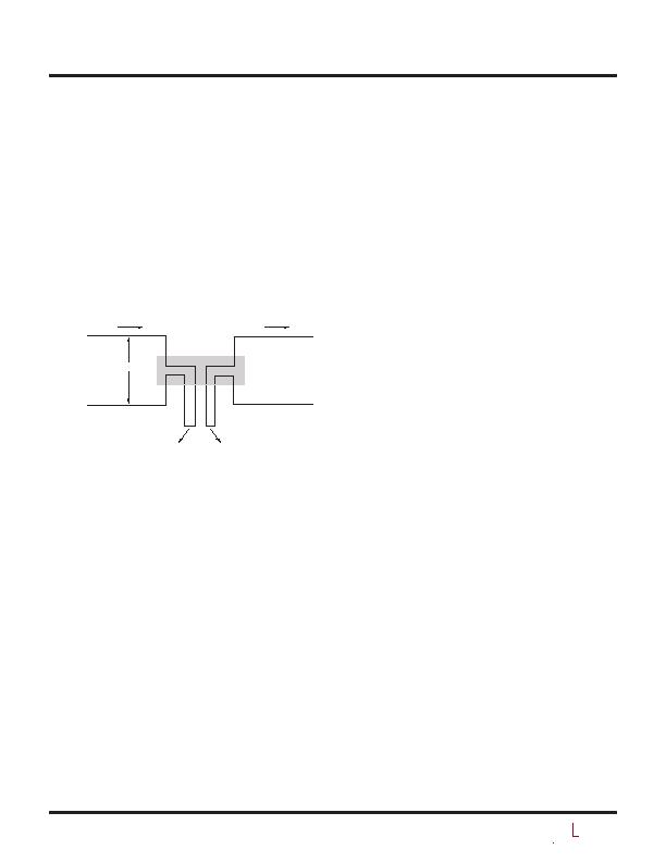
For proper circuit breaker operation, Kelvin-sense PCB
connections between the sense resistor and the LTC4253/
LTC4253As V
EE
and SENSE pins are strongly recom-
mended. The drawing in Figure 7 illustrates the correct way
of making connections between the LTC4253/LTC4253A
and the sense resistor. PCB layout should be balanced
and symmetrical to minimize wiring errors. In addition,
the PCB layout for the sense resistor should include good
thermal management techniques for optimal sense resistor
power dissipation.
Figure 7. Making PCB Connections to the Sense Resistor
TIMING WAVEFORMS
System Power-Up
Figure 8 details the timing waveforms for a typical power-
up sequence in the case where a board is already installed
in the backplane and system power is applied abruptly. At
time point 1, the supply ramps up, together with UV/OV ,
V
OUT
and DRAIN. V
IN
and the PWRGD signals follow at
a slower rate as set by the V
IN
bypass capacitor. At time
point 2, V
IN
exceeds V
LKO
and the internal logic checks for
UV > V
UVHI
(V
UV
for the LTC4253A), OV < V
OVLO
(V
OV
V
OVHST
for the LTC4253A), RESET < 0.8V , GATE < V
GATEL
,
SENSE < V
CB
, SS < 20 " V
OS
, and TIMER < V
TMRL
. When
all conditions are met, initial timing starts and the TIMER
capacitor is charged by a 5礎 current source pull-up. At
time point 3, TIMER reaches the V
TMRH
threshold and
the initial timing cycle terminates. The TIMER capacitor
is quickly discharged. At time point 4, the V
TMRL
thresh-
old is reached and the conditions of GATE < V
GATEL
,
SENSE?燰
CB
and SS < 20 " V
OS
must be satisfied before
the GATE start-up cycle begins. SS ramps up as dictated
by R
SS
" C
SS
(as in Equation 6); GATE is held low by the
analog current limit (ACL) amplifier until SS crosses 20 "
V
OS
. Upon releasing GATE, 50礎 sources into the external
MOSFET gate and compensation network. When the GATE
voltage reaches the MOSFETs threshold, current flows
into the load capacitor at time point 5. At time point 6,
load current reaches SS control level and the analog cur-
rent limit loop activates. Between time points 6 and 8, the
GATE voltage is servoed, the SENSE voltage is regulated
at V
ACL
(t) (Equation 7) and soft-start limits the slew rate
of the load current. If the SENSE voltage (V
SENSE
V
EE
)
reaches the V
CB
threshold at time point 7, circuit breaker
TIMER activates. The TIMER capacitor, C
T
, is charged by
a (200礎???營
DRN
) current pull-up. As the load capaci-
tor nears full charge, load current begins to decline. At
time point 8, the load current falls and the SENSE voltage
drops below V
ACL
(t). The analog current limit loop shuts
off and the GATE pin ramps further. At time point 9, the
SENSE voltage drops below V
CB
, the fault TIMER ends,
followed by a 5礎 discharge cycle (cool-off). The duration
between time points 7 and 9 must be shorter than one
circuit breaker delay to avoid fault time-out during GATE
ramp-up. When GATE ramps past the V
GATEH
threshold
at time point燗, PWRGD1 pulls low. At time point B, GATE
reaches its maximum voltage as determined by V
IN
. At time
point A, SQTIMER starts its ramp-up to 4V . Having satis-
fied the requirement that PWRGD1 is low for more than
one t
SQT
, PWRGD2 pulls low after EN2 pulls high above
the V
IH
threshold at time point C. This sets off the second
SQTIMER ramp-up. Having satisfied the requirement that
PWRGD2 is low for more than one t
SQT
, PWRGD3 pulls
low after EN3 pulls high at time point D.
W
CURRENT FLOW
FROM LOAD
CURRENT FLOW
TO 48V BACKPLANE
SENSE RESISTOR
TRACK WIDTH W:
0.03" PER AMP
ON 1 OZ COPPER
TO
SENSE
TO
V
EE
4253 F07
相关PDF资料 |
PDF描述 |
|---|---|
| MIC3775-1.5BMM TR | IC REG LDO 1.5V .75A 8-MSOP |
| EBM22DRXS | CONN EDGECARD 44POS DIP .156 SLD |
| TOP225YN | IC OFFLINE SWIT PWM OCP HV TO220 |
| ESA43DRMD | CONN EDGECARD 86POS .125 SQ WW |
| ECM12DRXI | CONN EDGECARD 24POS DIP .156 SLD |
相关代理商/技术参数 |
参数描述 |
|---|---|
| AD760AN | 制造商:未知厂家 制造商全称:未知厂家 功能描述:16-Bit Digital-to-Analog Converter |
| AD760AP | 制造商:未知厂家 制造商全称:未知厂家 功能描述:16-Bit Digital-to-Analog Converter |
| AD760AQ | 功能描述:IC DAC 16BIT W/AMP SRL 28-CDIP RoHS:否 类别:集成电路 (IC) >> 数据采集 - 数模转换器 系列:DACPORT® 产品培训模块:Lead (SnPb) Finish for COTS Obsolescence Mitigation Program 标准包装:50 系列:- 设置时间:4µs 位数:12 数据接口:串行 转换器数目:2 电压电源:单电源 功率耗散(最大):- 工作温度:-40°C ~ 85°C 安装类型:表面贴装 封装/外壳:8-TSSOP,8-MSOP(0.118",3.00mm 宽) 供应商设备封装:8-uMAX 包装:管件 输出数目和类型:2 电压,单极 采样率(每秒):* 产品目录页面:1398 (CN2011-ZH PDF) |
| AD760SQ | 制造商:未知厂家 制造商全称:未知厂家 功能描述:16-Bit Digital-to-Analog Converter |
| AD7610 | 制造商:AD 制造商全称:Analog Devices 功能描述:14-Bit, 1 MSPS, Differential, Programmable Input PulSAR ADC |
发布紧急采购,3分钟左右您将得到回复。