- 您现在的位置:买卖IC网 > PDF目录8616 > AD7808BRZ-REEL (Analog Devices Inc)IC DAC 10BIT OCTAL SRL 24-SOIC PDF资料下载
参数资料
| 型号: | AD7808BRZ-REEL |
| 厂商: | Analog Devices Inc |
| 文件页数: | 11/28页 |
| 文件大小: | 0K |
| 描述: | IC DAC 10BIT OCTAL SRL 24-SOIC |
| 产品培训模块: | Data Converter Fundamentals DAC Architectures |
| 标准包装: | 1,000 |
| 设置时间: | 1.5µs |
| 位数: | 10 |
| 数据接口: | 串行 |
| 转换器数目: | 4 |
| 电压电源: | 模拟和数字 |
| 功率耗散(最大): | 99mW |
| 工作温度: | -40°C ~ 85°C |
| 安装类型: | 表面贴装 |
| 封装/外壳: | 24-SOIC(0.295",7.50mm 宽) |
| 供应商设备封装: | 24-SOIC W |
| 包装: | 带卷 (TR) |
| 输出数目和类型: | 8 电压,双极 |
| 采样率(每秒): | 667k |
第1页第2页第3页第4页第5页第6页第7页第8页第9页第10页当前第11页第12页第13页第14页第15页第16页第17页第18页第19页第20页第21页第22页第23页第24页第25页第26页第27页第28页
AD7804/AD7805/AD7808/AD7809
–19–
REV. A
Table IX. Offset Binary Code Table for Sub DAC
Digital Input
Analog Output
MSB . . . LSB
11111111
VBIAS/16
× 127/256
11111110
VBIAS/16
× 126/256
10000001
VBIAS/16
× 1/256
10000000
0
01111111
–VBIAS/16
× 1/256
00000001
–VBIAS/16
× 127/256
00000000
–VBIAS/32
127
VBIAS
128
32
VBIAS
32
0
DAC
OUTPUT
VOLTAGE
00
01
DAC INPUT CODE
7F
80
81
FE
FF
Figure 26. Sub DAC Output Voltage vs. DAC Input Codes
(HEX) for Offset Binary Coding
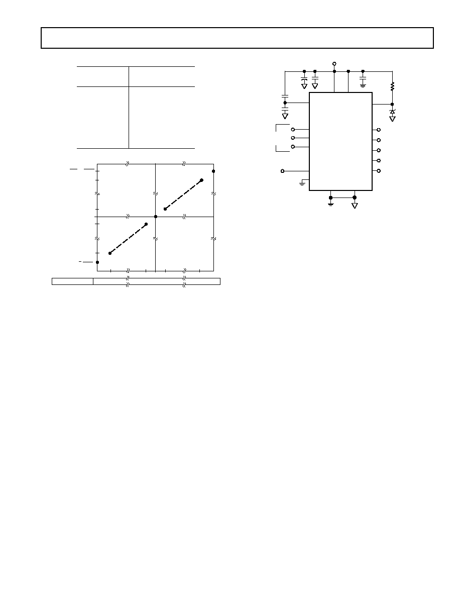
Configuring the AD7804/AD7808 for Offset Binary Coding
Figure 27 shows a typical configuration for the AD7804/AD7808.
This circuit can be used for both 3.3 V or 5 V operation and
uses an external AD589 as the reference for the part and serial
interfacing with offset binary coding is used. The MX1 and
MX0 bits in the system control register have to be set to enable
selection of the AD589 as the reference. The following are the
steps required to operate the DACs in this part. Figures 4 to 7
show the contents of the registers on the AD7804/AD7808.
AD589
0.01 F
AD7804/
AD7808
AVDD
DVDD
VOUTA
VOUTB
VOUTC
VOUTD
AGND
DGND
LDAC
CLR
COMP
SDIN
FSIN
DVDD
REFIN
REFOUT
0.1 F
10 F
0.01 F
SERIAL
INTERFACE
+3.3V/+5V
6.8k
CLKIN
Figure 27. Typical Configuration for AD7804/AD7808
Using an AD589 1.23 V Reference for the AD7804/AD7808
System Control Register Serial Write:
Write 0060 Hex
Mode bits select system control register
and configure system for offset binary
coding and normal operation.
Channel Control Register Serial Write:
Write 4210 Hex
Mode bits select channel control register,
channel A is configured for operation with
external reference.
Main DAC Data Register Serial Write:
Write 23FF Hex
This 16-bit write selects writing to channel
A and writes full scale to the Main DAC.
Sub DAC Data Register Serial Write:
Write A3FF Hex
This 16-bit write selects writing to channel
A Sub DAC and writes full scale to the
Sub DAC.
Table VIII and Figure 25 show the analog outputs available for
the above configuration when writing to the Main DAC only
while Table IX and Figure 26 show the contributions from the
Sub DAC to the overall transfer function. The total output for a
single channel when using offset binary coding is the sum of that
from the Main DAC and the Sub DAC.
VOUT = VOUT' + VOUT"
= VBIAS + 1.875
× V
BIAS
× ((NA-512)/1024) + V
BIAS/16
=
× [(NB-128)/256]
= VBIAS
× (1 + 1.875 × ((NA-512)/1024) + (NB-128)/
4096)
where NA ranges from 0 to +1023 and NB ranges from 0 to
+255. Figure 28 shows a pictorial view of the transfer function
for any DAC channel.
相关PDF资料 |
PDF描述 |
|---|---|
| VI-J6J-MW-S | CONVERTER MOD DC/DC 36V 100W |
| LT1567IMS8 | IC BLOCK BUILD FLTR LONOIS 8MSOP |
| VI-J6B-MW-S | CONVERTER MOD DC/DC 95V 100W |
| VI-25X-IV-F3 | CONVERTER MOD DC/DC 5.2V 150W |
| VI-25X-IV-F2 | CONVERTER MOD DC/DC 5.2V 150W |
相关代理商/技术参数 |
参数描述 |
|---|---|
| AD7808BST | 制造商:AD 制造商全称:Analog Devices 功能描述:+3.3 V to +5 V Quad/Octal 10-Bit DACs(300.12 k) |
| AD7809 | 制造商:AD 制造商全称:Analog Devices 功能描述:+3.3 V to +5 V Quad/Octal 10-Bit DACs |
| AD7809BST | 制造商:Analog Devices 功能描述:DAC 8-CH 10-bit 44-Pin TQFP 制造商:Rochester Electronics LLC 功能描述:OCTAL 10-BIT PARALLEL DAC I.C. - Bulk 制造商:Analog Devices 功能描述:IC 10-BIT DAC |
| AD7809BST-REEL | 制造商:Analog Devices 功能描述:DAC 8-CH 10-bit 44-Pin TQFP T/R |
发布紧急采购,3分钟左右您将得到回复。