- 您现在的位置:买卖IC网 > PDF目录10331 > AD7927WYRUZ-REEL7 (Analog Devices Inc)IC ADC 12BIT 8CH W/SEQ 20TSSOP PDF资料下载
参数资料
| 型号: | AD7927WYRUZ-REEL7 |
| 厂商: | Analog Devices Inc |
| 文件页数: | 11/28页 |
| 文件大小: | 0K |
| 描述: | IC ADC 12BIT 8CH W/SEQ 20TSSOP |
| 标准包装: | 1 |
| 位数: | 12 |
| 采样率(每秒): | 200k |
| 数据接口: | DSP,MICROWIRE?,QSPI?,串行,SPI? |
| 转换器数目: | 1 |
| 功率耗散(最大): | 7.5mW |
| 电压电源: | 单电源 |
| 安装类型: | 表面贴装 |
| 封装/外壳: | 20-TSSOP(0.173",4.40mm 宽) |
| 供应商设备封装: | 20-TSSOP |
| 包装: | 标准包装 |
| 输入数目和类型: | 8 个单端,单极 |
| 其它名称: | AD7927WYRUZ-REEL7DKR |
第1页第2页第3页第4页第5页第6页第7页第8页第9页第10页当前第11页第12页第13页第14页第15页第16页第17页第18页第19页第20页第21页第22页第23页第24页第25页第26页第27页第28页
Data Sheet
AD7927
Rev. D | Page 19 of 28
MODES OF OPERATION
The AD7927 has a number of different modes of operation,
which are designed to provide flexible power management
options. These options can be chosen to optimize the power
dissipation/throughput rate ratio for differing application
requirements. The mode of operation of the AD7927 is con-
trolled by the power management bits, PM1 and PM0, in the
control register, as detailed in Table 8. When power supplies
are first applied to the AD7927, care should be taken to ensure
that the part is placed in the required mode of operation (see
the Powering Up the AD7927 section).
NORMAL MODE (PM1 = PM0 = 1)
This mode is intended for the fastest throughput rate perform-
ance because the user does not have to worry about any power-
up times with the AD7927 remaining fully powered at all times.
Figure 21 shows the general diagram of the operation of the
AD7927 in this mode.
The conversion is initiated on the falling edge of CS and the track-
and-hold enters hold mode as described in the Serial Interface
section. The data presented to the AD7927 on the DIN line
during the first 12 clock cycles of the data transfer are loaded
into the control register (provided the WRITE bit is 1). If data is
to be written to the shadow register (SEQ = 0, SHADOW = 1 on
the previous write), data presented on the DIN line during the
first 16 SCLK cycles is loaded into the shadow register. The part
remains fully powered up in normal mode at the end of the
conversion as long as PM1 and PM0 are set to 1 in the write
transfer during that conversion. To ensure continued operation
in normal mode, PM1 and PM0 are both loaded with 1 on
every data transfer. Sixteen serial clock cycles are required to
complete the conversion and access the conversion result. The
track-and-hold goes back into track on the 14th SCLK falling
edge. CS may then idle high until the next conversion or may
idle low until sometime prior to the next conversion (effectively
idling CS low).
For specified performance, the throughput rate should not
exceed 200 kSPS, which means there should be no less than
5 μs between consecutive falling edges of CS when converting.
The actual frequency of SCLK used determines the duration of
the conversion within this 5 μs cycle; however, once a conversion
is complete and CS has returned high, a minimum of the quiet
time, tQUIET, must elapse before bringing CS low again to initiate
another conversion.
1
12
SCLK
DOUT
DIN
16
1 LEADING ZERO + 3 CHANNEL IDENTIFIER BITS
+ CONVERSION RESULT
DATA INTO CONTROL REGISTER/
SHADOW REGISTER
NOTES
1. CONTROL REGISTER DATA IS LOADED ON FIRST 12 SCLK CYCLES.
2. SHADOW REGISTER DATA IS LOADED ON FIRST 16 SCLK CYCLES.
CS
03
08
8-
02
1
Figure 21. Normal Mode Operation
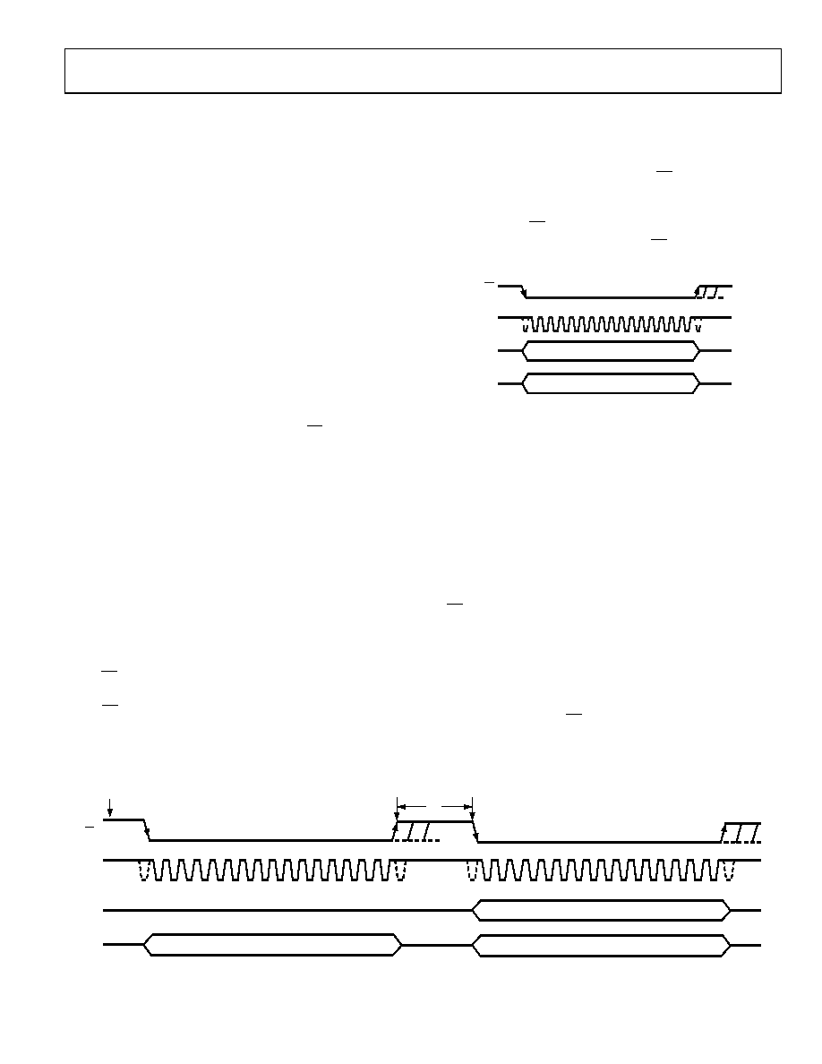
FULL SHUTDOWN (PM1 = 1, PM0 = 0)
In this mode, all internal circuitry on the AD7927 is powered
down. The part retains information in the control register during
full shutdown. The AD7927 remains in full shutdown until the
power management bits, PM1 and PM0, in the control register
are changed.
If a write to the control register occurs while the part is in full
shutdown, with the power management bits changed to PM0 =
CS rising edge. The track-and-hold that was in hold while the
part was in full shutdown returns to track on the 14th SCLK
falling edge. A full 16-SCLK transfer must occur to ensure the
control register contents are updated; however, the DOUT line
is not driven during this wake-up transfer.
To ensure that the part is fully powered up, tPOWER UP should have
elapsed before the next CS falling edge; otherwise, invalid data
is read if a conversion is initiated before this time. Figure 22 shows
the general diagram for this sequence.
SCLK
DOUT
DIN
1
CHANNEL IDENTIFIER BITS + CONVERSION RESULT
PART BEGINSTO POWER UP ON
CS RISING EDGE AS PM1 = PM0 = 1
THE PART IS FULLY POWERED UP
ONCE
tPOWER UP HAS ELAPSED
t12
14
16
14
16
DATA INTO CONTROL REGISTER/SHADOW REGISTER
TO KEEP THE PART IN NORMAL MODE, LOAD
PM1 = PM0 = 1 IN CONTROL REGISTER
DATA INTO CONTROL REGISTER
CONTROL REGISTER IS LOADED ON THE
FIRST 12 CLOCKS. PM1 = 1, PM0 = 1
PART IS IN FULL
SHUTDOWN
CS
03088
-022
Figure 22. Full Shutdown Mode Operation
相关PDF资料 |
PDF描述 |
|---|---|
| D38999/20WE8BA | CONN HSG RCPT 8POS WALL MT SCKT |
| D38999/26WG39SNLC | CONN HSG PLUG 39POS STRGHT SCKT |
| AD7789BRMZ-REEL | IC ADC 24BIT SIGMA-DELTA 10MSOP |
| D38999/26WC98SBLC | CONN HSG PLUG 10POS STRGHT SCKT |
| AD7790BRMZ-REEL | IC ADC 16BIT SIGMA-DELTA 10-MSOP |
相关代理商/技术参数 |
参数描述 |
|---|---|
| AD7928 | 制造商:AD 制造商全称:Analog Devices 功能描述:8-Channel, 1 MSPS, 8-/10-/12-Bit ADCs with Sequencer in 20-Lead TSSOP |
| AD7928BRU | 制造商:Analog Devices 功能描述:IC 12BIT ADC SMD 7928 TSSOP8 |
| AD7928BRU-REEL | 制造商:Analog Devices 功能描述:ADC Single SAR 1Msps 12-bit Serial 20-Pin TSSOP T/R |
| AD7928BRU-REEL7 | 制造商:Analog Devices 功能描述:ADC Single SAR 1Msps 12-bit Serial 20-Pin TSSOP T/R 制造商:Rochester Electronics LLC 功能描述:12-BIT 8, CH 1 MSPS ADC I.C. - Tape and Reel |
| AD7928BRUZ | 功能描述:IC ADC 12BIT 8CH 1MSPS 20-TSSOP RoHS:是 类别:集成电路 (IC) >> 数据采集 - 模数转换器 系列:- 标准包装:1 系列:microPOWER™ 位数:8 采样率(每秒):1M 数据接口:串行,SPI? 转换器数目:1 功率耗散(最大):- 电压电源:模拟和数字 工作温度:-40°C ~ 125°C 安装类型:表面贴装 封装/外壳:24-VFQFN 裸露焊盘 供应商设备封装:24-VQFN 裸露焊盘(4x4) 包装:Digi-Reel® 输入数目和类型:8 个单端,单极 产品目录页面:892 (CN2011-ZH PDF) 其它名称:296-25851-6 |
发布紧急采购,3分钟左右您将得到回复。