- 您现在的位置:买卖IC网 > PDF目录4105 > IDT7134LA20JG8 (IDT, Integrated Device Technology Inc)IC SRAM 32KBIT 20NS 52PLCC PDF资料下载
参数资料
| 型号: | IDT7134LA20JG8 |
| 厂商: | IDT, Integrated Device Technology Inc |
| 文件页数: | 9/12页 |
| 文件大小: | 0K |
| 描述: | IC SRAM 32KBIT 20NS 52PLCC |
| 标准包装: | 400 |
| 格式 - 存储器: | RAM |
| 存储器类型: | SRAM - 双端口,异步 |
| 存储容量: | 32K (4K x 8) |
| 速度: | 20ns |
| 接口: | 并联 |
| 电源电压: | 4.5 V ~ 5.5 V |
| 工作温度: | 0°C ~ 70°C |
| 封装/外壳: | 52-LCC(J 形引线) |
| 供应商设备封装: | 52-PLCC(19x19) |
| 包装: | 带卷 (TR) |
| 其它名称: | 7134LA20JG8 |
�� �
�
�IDT7134SA/LA�
�High-Speed� 4K� x� 8� Dual-Port� Static� SRAM�
�Military,� Industrial� and� Commercial� Temperature� Ranges�
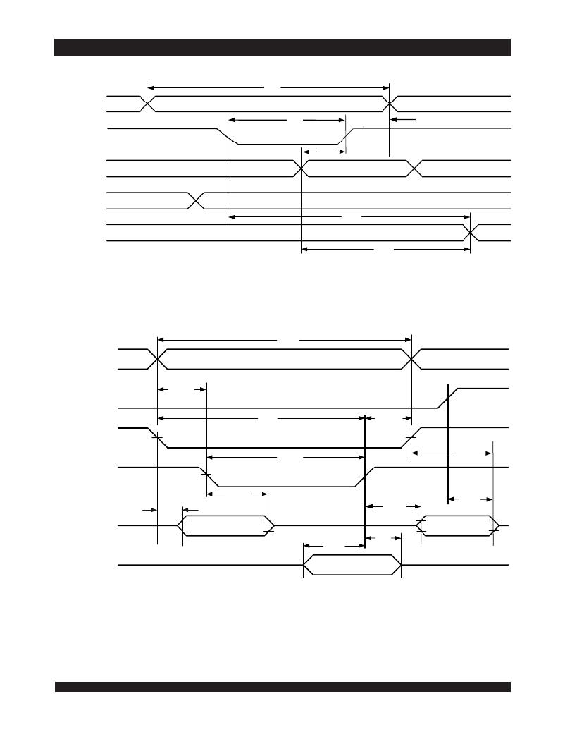
�Timing� Waveform� of� Write� with� Port-to-Port� Read� (1,2,3)�
�t� WC�
�ADDR� "A"�
�MATCH�
�R/� W� "A"�
�DATA� IN� "A"�
�ADDR� "B"�
�DATA� OUT� "B"�
�(1)�
�t� WP�
�t� DW�
�VALID�
�MATCH�
�t� WDD�
�t� AW�
�VALID�
�NOTES:�
�t� DDD�
�2720� drw� 10�
�1.� Write� cycle� parameters� should� be� adhered� to,� in� order� to� ensure� proper� writing.�
�2.� CE� L� =� CE� R� =� V� IL.� OE� "B"� =� V� IL.�
�3.� Port� "A"� may� be� either� left� or� right� port.� Port� "B"� is� the� opposite� from� port� "A".�
�Timing� Waveform� of� Write� Cycle� No.� 1,� R/� W� Controlled� Timing� (1,5,8)�
�t� WC�
�ADDRESS�
�OE�
�t� AS� (6)�
�CE�
�R/� W�
�t� AW�
�t� WP� (2)�
�t� WR� (3)�
�t� HZ� (7)�
�t� LZ�
�DATA� OUT�
�(7)�
�t� WZ� (7)�
�(4)�
�t� DW�
�t� OW�
�t� DH�
�t� HZ� (7)�
�(4)�
�DATA� IN�
�NOTES:�
�2720� drw� 11�
�1.� R/� W� or� CE� must� be� HIGH� during� all� address� transitions.�
�2.� A� write� occurs� during� the� overlap� (t� EW� or� t� WP� )� of� a� CE� =V� IL� and� R/� W� =� V� IL� .�
�3.� t� WR� is� measured� from� the� earlier� of� CE� or� R/� W� going� to� V� IH� to� the� end-of-write� cycle.�
�4.� During� this� period,� the� I/O� pins� are� in� the� output� state,� and� input� signals� must� not� be� applied.�
�5.� If� the� CE� =� V� IL� transition� occurs� simultaneously� with� or� after� the� R/� W� =� V� IL� transition,� the� outputs� remain� in� the� High-impedance� state.�
�6.� Timing� depends� on� which� enable� signal� (� CE� or� R/� W� )� is� asserted� last.�
�7.� This� parameter� is� guaranteed� by� device� characterization,� but� is� not� production� tested.� Transition� is� measured� 0mV� from� steady� state� with� the� Output� Test� Load�
�(Figure� 2).�
�8.� If� OE� =� V� IL� during� a� R/� W� controlled� write� cycle,� the� write� pulse� width� must� be� the� larger� of� t� WP� or� (t� WZ� +� t� DW� )� to� allow� the� I/O� drivers� to� turn� off� data� to� be� placed� on� the� bus�
�for� the� required� t� DW� .� If� OE� =� V� IH� during� an� R� /W� controlled� write� cycle,� this� requirement� does� not� apply� and� the� write� pulse� can� be� as� short� as� the� specified� t� WP� .�
�9�
�相关PDF资料 |
PDF描述 |
|---|---|
| 4-1734839-8 | CONN FPC 48POS .5MM RT ANG SMD |
| IDT7134LA20J8 | IC SRAM 32KBIT 20NS 52PLCC |
| MPC8260AVVMHBB | IC MPU POWERQUICC II 480-TBGA |
| IDT71342LA20JG8 | IC SRAM 32KBIT 20NS 52PLCC |
| MPC8260AZUMHBB | IC MPU POWERQUICC II 480-TBGA |
相关代理商/技术参数 |
参数描述 |
|---|---|
| AD8220BRMZ | 功能描述:IC AMP INST JFET R-R 15MA 8MSOP RoHS:是 类别:集成电路 (IC) >> Linear - Amplifiers - Instrumentation 系列:- 标准包装:2,500 系列:- 放大器类型:通用 电路数:4 输出类型:- 转换速率:0.6 V/µs 增益带宽积:1MHz -3db带宽:- 电流 - 输入偏压:45nA 电压 - 输入偏移:2000µV 电流 - 电源:1.4mA 电流 - 输出 / 通道:40mA 电压 - 电源,单路/双路(±):3 V ~ 32 V,±1.5 V ~ 16 V 工作温度:0°C ~ 70°C 安装类型:表面贴装 封装/外壳:14-TSSOP(0.173",4.40mm 宽) 供应商设备封装:14-TSSOP 包装:带卷 (TR) 其它名称:LM324ADTBR2G-NDLM324ADTBR2GOSTR |
| AD8220BRMZ-R7 | 功能描述:IC AMP INST JFET R-R 15MA 8MSOP RoHS:是 类别:集成电路 (IC) >> Linear - Amplifiers - Instrumentation 系列:- 标准包装:50 系列:- 放大器类型:J-FET 电路数:2 输出类型:- 转换速率:13 V/µs 增益带宽积:3MHz -3db带宽:- 电流 - 输入偏压:65pA 电压 - 输入偏移:3000µV 电流 - 电源:1.4mA 电流 - 输出 / 通道:- 电压 - 电源,单路/双路(±):7 V ~ 36 V,±3.5 V ~ 18 V 工作温度:-40°C ~ 85°C 安装类型:通孔 封装/外壳:8-DIP(0.300",7.62mm) 供应商设备封装:8-PDIP 包装:管件 |
| AD8220BRMZ-RL | 功能描述:IC AMP INST JFET R-R 15MA 8MSOP RoHS:是 类别:集成电路 (IC) >> Linear - Amplifiers - Instrumentation 系列:- 标准包装:50 系列:- 放大器类型:J-FET 电路数:2 输出类型:- 转换速率:13 V/µs 增益带宽积:3MHz -3db带宽:- 电流 - 输入偏压:65pA 电压 - 输入偏移:3000µV 电流 - 电源:1.4mA 电流 - 输出 / 通道:- 电压 - 电源,单路/双路(±):7 V ~ 36 V,±3.5 V ~ 18 V 工作温度:-40°C ~ 85°C 安装类型:通孔 封装/外壳:8-DIP(0.300",7.62mm) 供应商设备封装:8-PDIP 包装:管件 |
| AD8220-EVAL | 制造商:AD 制造商全称:Analog Devices 功能描述:JFET Input Instrumentation Amplifier with Rail-to-Rail Output in MSOP Package |
| AD8220-EVALZ | 制造商:Analog Devices 功能描述:Evaluation Board For JFET Instrumentation Amplifier Evaluation Board 制造商:Analog Devices 功能描述:JFET INSTRUMENTATION AMP EVAL BD - Bulk 制造商:Analog Devices 功能描述:AD8220 Evaluation Board |
发布紧急采购,3分钟左右您将得到回复。