- 您现在的位置:买卖IC网 > PDF目录9355 > DS17485SN-5+ (Maxim Integrated Products)IC RTC 5V 4K NV RAM 24-SOIC PDF资料下载
参数资料
| 型号: | DS17485SN-5+ |
| 厂商: | Maxim Integrated Products |
| 文件页数: | 16/31页 |
| 文件大小: | 0K |
| 描述: | IC RTC 5V 4K NV RAM 24-SOIC |
| 产品培训模块: | Lead (SnPb) Finish for COTS Obsolescence Mitigation Program |
| 标准包装: | 31 |
| 类型: | 时钟/日历 |
| 特点: | 警报器,夏令时,闰年,NVSRAM,方波输出 |
| 存储容量: | 4KB |
| 时间格式: | HH:MM:SS(12/24 小时) |
| 数据格式: | YY-MM-DD-dd |
| 接口: | 并联 |
| 电源电压: | 4.5 V ~ 5.5 V |
| 电压 - 电源,电池: | 2.5 V ~ 3.7 V |
| 工作温度: | -40°C ~ 85°C |
| 安装类型: | 表面贴装 |
| 封装/外壳: | 24-SOIC(0.295",7.50mm 宽) |
| 供应商设备封装: | 24-SOIC W |
| 包装: | 管件 |
第1页第2页第3页第4页第5页第6页第7页第8页第9页第10页第11页第12页第13页第14页第15页当前第16页第17页第18页第19页第20页第21页第22页第23页第24页第25页第26页第27页第28页第29页第30页第31页
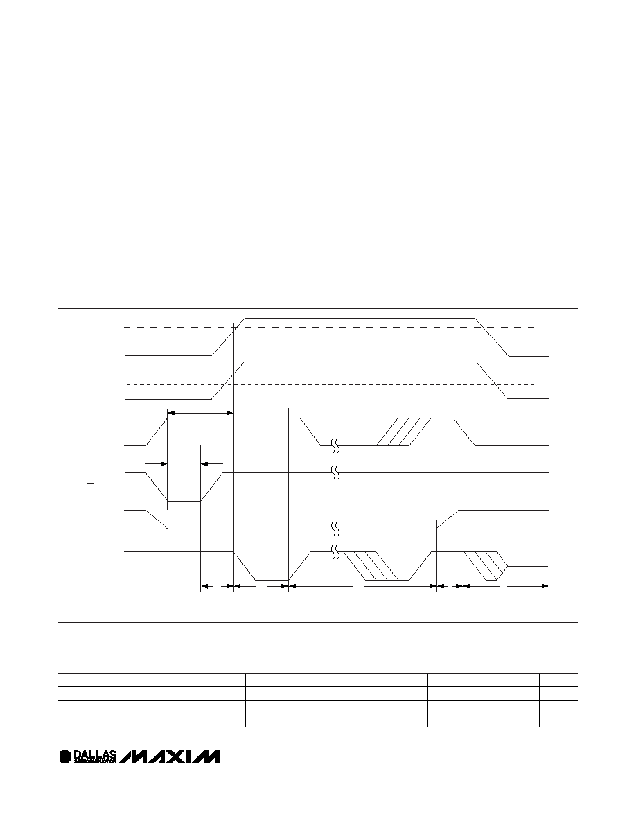
The timing associated with both the wake-up and kick-
starting sequences is illustrated in the
Wake-
Up/Kickstart Timing Diagram (Figure 6). The timing
associated with these functions is divided into five inter-
vals, labeled 1 to 5 on the diagram.
The occurrence of either a kickstart or wake-up condition
causes the PWR pin to be driven low, as described
above. During interval 1, if the supply voltage on the
DS17x85/DS17x87 VCC pin rises above the greater of
VBAT or VPF before the power-on timeout period (tPOTO)
expires, then PWR remains at the active-low level. If VCC
does not rise above the greater of VBAT or VPF in this
time, then the PWR output pin is turned off and returns to
its high-impedance level. In this event, the IRQ pin also
remains tri-stated. The interrupt flag bit (either WF or KF)
associated with the attempted power-on sequence
remains set until cleared by software during a subse-
quent system power-on.
If VCC is applied within the timeout period, then the sys-
tem power-on sequence continue as shown in intervals
2 to 5 in the timing diagram. During interval 2, PWR
remains active and IRQ is driven to its active-low level,
indicating that either WF or KF was set in initiating the
power-on. In the diagram KS is assumed to be pulled
up to the VBAUX supply. Also at this time, the PAB bit is
automatically cleared to 0 in response to a successful
power-on. The PWR line remains active as long as the
PAB remains cleared to 0.
DS17285/DS17287/DS17485/DS17487/DS17885/DS17887
Real-Time Clocks
____________________________________________________________________
23
Figure 6. Wake-Up/Kickstart Timing Diagram
Note: Wake-up/kickstart timeout is generated only when the oscillator is enabled and the countdown chain is not reset.
VBAT
VIH
tKSPW
tPOTP
VIH
1
2
3
45
VIL
HIGH-IMPEDANCE
VIL
VPF
0V
*CONDITION
VPF < VBAT
*THIS CONDITION CAN OCCUR WITH THE 3V DEVICE.
NOTE: THE TIME INTERVALS SHOWN ABOVE ARE REFERENCED IN THE WAKE-UP/KICKSTART SECTION.
*CONDITION
VBAT > VPF
WF/KF
(INTERNAL)
KS
PWR
IRQ
Table 6. Wake-Up/Kickstart Timing
(TA =+25°C)
PARAMETER
SYMBOL
CONDITIONS
MIN
TYP
MAX
UNITS
Kickstart-Input Pulse Width
tKSPW
2s
Wake-Up/Kickstart Power-On
Timeout
tPOTO
2s
相关PDF资料 |
PDF描述 |
|---|---|
| DS12885QN+ | IC RTC W/RAM 128 BYTE IND 28PLCC |
| MCP4131T-103E/SN | IC POT DGTL SNGL 10K SPI 8SOIC |
| DS12885SN+ | IC RTC W/RAM 128 BYTE IND 24SOIC |
| VI-B5D-IU-S | CONVERTER MOD DC/DC 85V 200W |
| DS17485S-5+ | IC RTC 5V 4K NV RAM 24-SOIC |
相关代理商/技术参数 |
参数描述 |
|---|---|
| AD8260-EVALZ | 功能描述:BOARD EVAL FOR AD8260 RoHS:是 类别:编程器,开发系统 >> 评估板 - 运算放大器 系列:- 产品培训模块:Lead (SnPb) Finish for COTS Obsolescence Mitigation Program 标准包装:1 系列:- |
| AD8264 | 制造商:AD 制造商全称:Analog Devices 功能描述:Quad, 235 MHz, DC-Coupled VGA and Differential Output Amplifier |
| AD8264ACPZ | 功能描述:IC AMP VGA DIFF QUAD LN 40LFCSP RoHS:是 类别:集成电路 (IC) >> Linear - Amplifiers - Instrumentation 系列:- 标准包装:1 系列:- 放大器类型:通用 电路数:4 输出类型:满摆幅 转换速率:0.028 V/µs 增益带宽积:105kHz -3db带宽:- 电流 - 输入偏压:3nA 电压 - 输入偏移:100µV 电流 - 电源:3.3µA 电流 - 输出 / 通道:12mA 电压 - 电源,单路/双路(±):2.7 V ~ 12 V,±1.35 V ~ 6 V 工作温度:-40°C ~ 85°C 安装类型:表面贴装 封装/外壳:14-TSSOP(0.173",4.40mm 宽) 供应商设备封装:14-TSSOP 包装:剪切带 (CT) 其它名称:OP481GRUZ-REELCT |
| AD8264ACPZ-R7 | 功能描述:IC AMP VGA DIFF QUAD LN 40LFCSP RoHS:是 类别:集成电路 (IC) >> Linear - Amplifiers - Instrumentation 系列:- 标准包装:50 系列:- 放大器类型:J-FET 电路数:2 输出类型:- 转换速率:3.5 V/µs 增益带宽积:1MHz -3db带宽:- 电流 - 输入偏压:30pA 电压 - 输入偏移:2000µV 电流 - 电源:200µA 电流 - 输出 / 通道:- 电压 - 电源,单路/双路(±):7 V ~ 36 V,±3.5 V ~ 18 V 工作温度:0°C ~ 70°C 安装类型:通孔 封装/外壳:8-DIP(0.300",7.62mm) 供应商设备封装:8-PDIP 包装:管件 |
| AD8264ACPZ-RL | 功能描述:IC AMP VGA DIFF QUAD LN 40LFCSP RoHS:是 类别:集成电路 (IC) >> Linear - Amplifiers - Instrumentation 系列:- 标准包装:2,500 系列:Excalibur™ 放大器类型:J-FET 电路数:1 输出类型:- 转换速率:45 V/µs 增益带宽积:10MHz -3db带宽:- 电流 - 输入偏压:20pA 电压 - 输入偏移:490µV 电流 - 电源:1.7mA 电流 - 输出 / 通道:48mA 电压 - 电源,单路/双路(±):4.5 V ~ 38 V,±2.25 V ~ 19 V 工作温度:-40°C ~ 85°C 安装类型:表面贴装 封装/外壳:8-SOIC(0.154",3.90mm 宽) 供应商设备封装:8-SOIC 包装:带卷 (TR) |
发布紧急采购,3分钟左右您将得到回复。