- 您现在的位置:买卖IC网 > PDF目录10215 > AD9214BRSZ-RL105 (Analog Devices Inc)IC ADC 10BIT 105MSPS 28-SSOP T/R PDF资料下载
参数资料
| 型号: | AD9214BRSZ-RL105 |
| 厂商: | Analog Devices Inc |
| 文件页数: | 5/20页 |
| 文件大小: | 0K |
| 描述: | IC ADC 10BIT 105MSPS 28-SSOP T/R |
| 标准包装: | 1,500 |
| 位数: | 10 |
| 采样率(每秒): | 105M |
| 数据接口: | 并联 |
| 转换器数目: | 1 |
| 功率耗散(最大): | 325mW |
| 电压电源: | 模拟和数字 |
| 工作温度: | -40°C ~ 85°C |
| 安装类型: | 表面贴装 |
| 封装/外壳: | 28-SSOP(0.209",5.30mm 宽) |
| 供应商设备封装: | 28-SSOP |
| 包装: | 带卷 (TR) |
| 输入数目和类型: | 2 个单端,单极;1 个差分,单极 |
REV. D
AD9214
–13–
AD9214
50
ANALOG
SIGNAL
SOURCE
15pF
50
VOCM
+
–
+
AD8138
500
0.1 F
AVDD
10k
5k
AIN
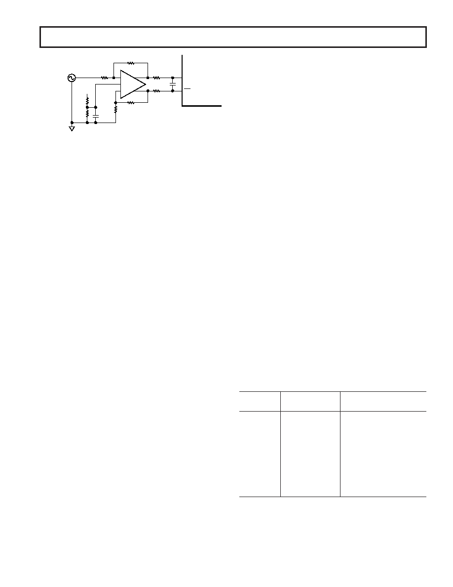
Figure 9. DC-Coupled Analog Input Circuit
POWER SUPPLIES
The AD9214 has two power supplies, AVDD and DrVDD. AVDD
and AGND supply power to all the analog circuitry, the inputs
and the internal timing and digital error correction circuits.
AVDD supply current will vary slightly with encode rate, as noted in
the Typical Performance Characteristics section.
DrVDD and DGND supply only the CMOS digital outputs,
allowing the user to adjust the voltage level to match down-
stream logic.
DrVDD current will vary depending on the voltage level, external
loading capacitance, and the encode frequency. Designs that mini-
mize external load capacitance will reduce power consumption
and reduce supply noise that may affect ADC performance. The
maximum DrVDD current can be calculated as
I
V
C
fencode
N
DrV
LOAD
DD
=×
×
where N is the number of output bits, 10 in the case of the
AD9214. This maximum current is for the condition of every
output bit switching on every clock cycle, which can only occur
for a full scale square wave at the Nyquist frequency, fENCODE /2.
In practice, IDrV
DD
will be the average number of output bits
switching, which will be determined by the encode rate and the
characteristics of the analog input signal. The performance
curves section provides a reference of IDrV
DD
versus encode rate
for a 10.3 MHz sine wave driving the analog input.
Both power supply connections should be decoupled to ground
at or near the package connections, using high quality, ceramic
chip capacitors. A single ground plane is recommended for all
ground (AGND and DGND) connections.
The PWRDN control pin configures the AD9214 for a sleep
mode when it is logic HIGH. PWRDN floats logic LOW for
normal operation. In sleep mode, the ADC is not active, and
will consume less power. When switching from sleep mode to
normal operation, the ADC will need ~15 clock cycles to recover to
valid output data.
Digital Outputs
Care must be taken when designing the data receivers for the
AD9214. It is recommended that the digital outputs drive a
series resistor (e.g., 100
) followed by a gate like the 74LCX821.
To minimize capacitive loading, there should be only one gate
on each output pin. An example of this is shown in the evaluation
board schematic in Figure 10. The series resistors should be
placed as close to the AD9214 as possible to limit the amount of
current that can flow into the output stage. These switching
currents are confined between ground (DGND) and the DrVDD
pins. Standard TTL gates should be avoided since they can
appreciably add to the dynamic switching currents of the AD9214.
It should also be noted that extra capacitive loading will increase
output timing and invalidate timing specifications. Digital output
timing is guaranteed with 10 pF loads.
LAYOUT INFORMATION
The schematic of the evaluation board (Figure 10) represents a
typical implementation of the AD9214. A multilayer board is
recommended to achieve best results. It is highly recommended
that high quality, ceramic chip capacitors be used to decouple
each supply pin to ground directly at the device. The pinout of
the AD9214 facilitates ease of use in the implementation of high
frequency, high resolution design practices. All of the digital
outputs and their supply and ground pin connections are segre-
gated to one side of the package, with the inputs on the opposite
side for isolation purposes.
Care should be taken when routing the digital output traces. To
prevent coupling through the digital outputs into the analog
portion of the AD9214, minimal capacitive loading should be
placed on these outputs. It is recommended that a fan-out of
only one gate should be used for all AD9214 digital outputs.
The layout of the encode circuit is equally critical. Any noise
received on this circuitry will result in corruption in the digitiza-
tion process and lower overall performance. The Encode clock
must be isolated from the digital outputs and the analog inputs.
EVALUATION BOARD
The AD9214 evaluation board offers designers an easy way to
evaluate device performance. The user must supply an analog
input signal, encode clock reference, and power supplies. The
digital outputs of the AD9214 are latched on the evaluation
board, and are available with a data ready signal at a 40-pin
edge connector. Please refer to the evaluation board schematic,
layout, and Bill of Materials.
Power Connections
Power to the board is supplied via three detachable, 4-pin power
strips (U4, U9, and U10). These 12 pins should be driven as
outlined in the Table II.
Table II. Power Supply Connections for AD9214
Evaluation Board
External Supply
Pin
Designator
Required
1
LVC
3 V
3
+5 V
(Optional Z1 Supply)
5
–5 V
(Optional Z1 Supply)
7
VCC
3 V
9
VDD
3 V
11
DAC
5 V
2, 4, 6,
GND
Ground
8, 10, 12
Please note that the +5 V and –5 V supplies are optional, and
only required if the user adds differential op amp Z1 to the board.
相关PDF资料 |
PDF描述 |
|---|---|
| VI-2NK-IW-S | CONVERTER MOD DC/DC 40V 100W |
| VI-B2N-MW-F2 | CONVERTER MOD DC/DC 18.5V 100W |
| D38999/20MC98SN | CONN RCPT 10POS WALL MNT W/SCKT |
| AD7472ARU | IC ADC 12BIT PARALLEL 24-TSSOP |
| VI-B2N-MW-F1 | CONVERTER MOD DC/DC 18.5V 100W |
相关代理商/技术参数 |
参数描述 |
|---|---|
| AD9214BRSZ-RL65 | 功能描述:IC ADC 10BIT 65MSPS 28-SSOP T/R RoHS:是 类别:集成电路 (IC) >> 数据采集 - 模数转换器 系列:- 标准包装:1,000 系列:- 位数:16 采样率(每秒):45k 数据接口:串行 转换器数目:2 功率耗散(最大):315mW 电压电源:模拟和数字 工作温度:0°C ~ 70°C 安装类型:表面贴装 封装/外壳:28-SOIC(0.295",7.50mm 宽) 供应商设备封装:28-SOIC W 包装:带卷 (TR) 输入数目和类型:2 个单端,单极 |
| AD9214BRSZ-RL80 | 功能描述:IC ADC 10BIT 80MSPS 28-SSOP T/R RoHS:是 类别:集成电路 (IC) >> 数据采集 - 模数转换器 系列:- 标准包装:1,000 系列:- 位数:12 采样率(每秒):300k 数据接口:并联 转换器数目:1 功率耗散(最大):75mW 电压电源:单电源 工作温度:0°C ~ 70°C 安装类型:表面贴装 封装/外壳:24-SOIC(0.295",7.50mm 宽) 供应商设备封装:24-SOIC 包装:带卷 (TR) 输入数目和类型:1 个单端,单极;1 个单端,双极 |
| AD9215 | 制造商:Analog Devices 功能描述:- Bulk |
| AD9215_13 | 制造商:AD 制造商全称:Analog Devices 功能描述:10-Bit, 65/80/105 MSPS, 3 V A/D Converter |
| AD9215BCP-105 | 制造商:Analog Devices 功能描述:ADC Single Pipelined 105Msps 10-bit Parallel 32-Pin LFCSP EP 制造商:Analog Devices 功能描述:10BIT ADC 105MSPS 9215 LFCSP-32 |
发布紧急采购,3分钟左右您将得到回复。