- 您现在的位置:买卖IC网 > PDF目录4076 > MPC857DSLVR50B (Freescale Semiconductor)IC MPU POWERQUICC 50MHZ 357-PBGA PDF资料下载
参数资料
| 型号: | MPC857DSLVR50B |
| 厂商: | Freescale Semiconductor |
| 文件页数: | 16/88页 |
| 文件大小: | 0K |
| 描述: | IC MPU POWERQUICC 50MHZ 357-PBGA |
| 标准包装: | 44 |
| 系列: | MPC8xx |
| 处理器类型: | 32-位 MPC8xx PowerQUICC |
| 速度: | 50MHz |
| 电压: | 3.3V |
| 安装类型: | 表面贴装 |
| 封装/外壳: | 357-BBGA |
| 供应商设备封装: | 357-PBGA(25x25) |
| 包装: | 托盘 |
第1页第2页第3页第4页第5页第6页第7页第8页第9页第10页第11页第12页第13页第14页第15页当前第16页第17页第18页第19页第20页第21页第22页第23页第24页第25页第26页第27页第28页第29页第30页第31页第32页第33页第34页第35页第36页第37页第38页第39页第40页第41页第42页第43页第44页第45页第46页第47页第48页第49页第50页第51页第52页第53页第54页第55页第56页第57页第58页第59页第60页第61页第62页第63页第64页第65页第66页第67页第68页第69页第70页第71页第72页第73页第74页第75页第76页第77页第78页第79页第80页第81页第82页第83页第84页第85页第86页第87页第88页
MPC862/857T/857DSL PowerQUICC Family Hardware Specifications, Rev. 3
Freescale Semiconductor
23
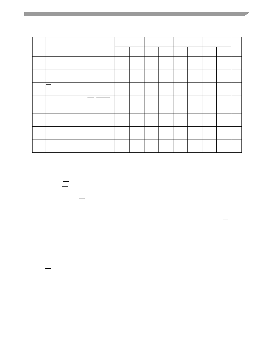
Bus Signal Timing
B37
UPWAIT valid to CLKOUT falling edge
12 (MIN = 0.00 x B1 + 6.00)
6.00
—
6.00
—
6.00
—
6.00
—
ns
B38
CLKOUT falling edge to UPWAIT valid
12 (MIN = 0.00 x B1 + 1.00)
1.00
—
1.00
—
1.00
—
1.00
—
ns
B39
AS valid to CLKOUT rising edge 13
(MIN = 0.00 x B1 + 7.00)
7.00
—
7.00
—
7.00
—
7.00
—
ns
B40
A(0:31), TSIZ(0:1), RD/WR, BURST,
valid to CLKOUT rising edge
(MIN = 0.00 x B1 + 7.00)
7.00
—
7.00
—
7.00
—
7.00
—
ns
B41
TS valid to CLKOUT rising edge (setup
time) (MIN = 0.00 x B1 + 7.00)
7.00
—
7.00
—
7.00
—
7.00
—
ns
B42
CLKOUT rising edge to TS valid (hold
time) (MIN = 0.00 x B1 + 2.00)
2.00
—
2.00
—
2.00
—
2.00
—
ns
B43
AS negation to memory controller
signals negation (MAX = TBD)
—
TBD
—
TBD
—
TBD
—
TBD
ns
1
Phase and frequency jitter performance results are only valid if the input jitter is less than the prescribed value.
2
If the rate of change of the frequency of EXTAL is slow (I.e. it does not jump between the minimum and maximum
values in one cycle) or the frequency of the jitter is fast (I.e., it does not stay at an extreme value for a long time) then
the maximum allowed jitter on EXTAL can be up to 2%.
3
The timings specified in B4 and B5 are based on full strength clock.
4
The timing for BR output is relevant when the MPC862/857T/857DSL is selected to work with external bus arbiter.
The timing for BG output is relevant when the MPC862/857T/857DSL is selected to work with internal bus arbiter.
5
For part speeds above 50MHz, use 9.80ns for B11a.
6
The timing required for BR input is relevant when the MPC862/857T/857DSL is selected to work with internal bus
arbiter. The timing for BG input is relevant when the MPC862/857T/857DSL is selected to work with external bus
arbiter.
7
For part speeds above 50MHz, use 2ns for B17.
8
The D(0:31) and DP(0:3) input timings B18 and B19 refer to the rising edge of the CLKOUT in which the TA input
signal is asserted.
9
For part speeds above 50MHz, use 2ns for B19.
10 The D(0:31) and DP(0:3) input timings B20 and B21 refer to the falling edge of the CLKOUT. This timing is valid only
for read accesses controlled by chip-selects under control of the UPM in the memory controller, for data beats where
DLT3 = 1 in the UPM RAM words. (This is only the case where data is latched on the falling edge of CLKOUT.)
11 The timing B30 refers to CS when ACS = 00 and to WE(0:3) when CSNT = 0.
12 The signal UPWAIT is considered asynchronous to the CLKOUT and synchronized internally. The timings specified
in B37 and B38 are specified to enable the freeze of the UPM output signals as described in Figure 19.
13 The AS signal is considered asynchronous to the CLKOUT. The timing B39 is specified in order to allow the behavior
specified in Figure 22.
Table 7. Bus Operation Timings (continued)
Num
Characteristic
33 MHz
40 MHz
50 MHz
66 MHz
Unit
Min
Max
Min
Max
Min
Max
Min
Max
相关PDF资料 |
PDF描述 |
|---|---|
| MPC8314EVRAFDA | MPU POWERQUICC II PRO 620-PBGA |
| MPC8314ECVRADDA | MPU POWERQUICC II PRO 620-PBGA |
| ASC60DRAI-S734 | CONN EDGECARD 120PS .100 R/A PCB |
| MPC8314CVRAFDA | MPU POWERQUICC II PRO 620-PBGA |
| MC68306EH16B | IC MPU INTEGRATED 16MHZ 132-PQFP |
相关代理商/技术参数 |
参数描述 |
|---|---|
| ADA4841-2YRZ-RL | 功能描述:IC OPAMP VF R-R DUAL LP LN 8SOIC RoHS:是 类别:集成电路 (IC) >> Linear - Amplifiers - Instrumentation 系列:- 产品培训模块:Lead (SnPb) Finish for COTS Obsolescence Mitigation Program 标准包装:1 系列:- 放大器类型:电流检测 电路数:1 输出类型:- 转换速率:- 增益带宽积:125kHz -3db带宽:- 电流 - 输入偏压:- 电压 - 输入偏移:100µV 电流 - 电源:1.1µA 电流 - 输出 / 通道:- 电压 - 电源,单路/双路(±):- 工作温度:-40°C ~ 85°C 安装类型:表面贴装 封装/外壳:4-WFBGA,CSPBGA 供应商设备封装:4-UCSP(2x2) 包装:剪切带 (CT) 其它名称:MAX9634WERS+TCT |
| ADA4841-X | 制造商:AD 制造商全称:Analog Devices 功能描述:14-Bit, 8-Channel, 250 kSPS PulSAR ADC |
| ADA4850-1 | 制造商:AD 制造商全称:Analog Devices 功能描述:High Speed, Rail-to-Rail Output Op Amps with Ultralow Power-Down |
| ADA4850-1_07 | 制造商:AD 制造商全称:Analog Devices 功能描述:High Speed, Rail-to-Rail Output Op Amps with Ultralow Power-Down |
| ADA4850-1YCPZ-R2 | 功能描述:IC OPAMP VF R-R 118MA 8LFCSP RoHS:是 类别:集成电路 (IC) >> Linear - Amplifiers - Instrumentation 系列:- 标准包装:1 系列:- 放大器类型:通用 电路数:4 输出类型:满摆幅 转换速率:0.028 V/µs 增益带宽积:105kHz -3db带宽:- 电流 - 输入偏压:3nA 电压 - 输入偏移:100µV 电流 - 电源:3.3µA 电流 - 输出 / 通道:12mA 电压 - 电源,单路/双路(±):2.7 V ~ 12 V,±1.35 V ~ 6 V 工作温度:-40°C ~ 85°C 安装类型:表面贴装 封装/外壳:14-TSSOP(0.173",4.40mm 宽) 供应商设备封装:14-TSSOP 包装:剪切带 (CT) 其它名称:OP481GRUZ-REELCT |
发布紧急采购,3分钟左右您将得到回复。