- 您现在的位置:买卖IC网 > PDF目录374016 > ADMC401BST (ANALOG DEVICES INC) Single-Chip, DSP-Based High Performance Motor Controller PDF资料下载
参数资料
| 型号: | ADMC401BST |
| 厂商: | ANALOG DEVICES INC |
| 元件分类: | 数字信号处理 |
| 英文描述: | Single-Chip, DSP-Based High Performance Motor Controller |
| 中文描述: | 24-BIT, 13 MHz, OTHER DSP, PQFP144 |
| 封装: | PLASTIC, LQFP-144 |
| 文件页数: | 20/60页 |
| 文件大小: | 417K |
| 代理商: | ADMC401BST |
第1页第2页第3页第4页第5页第6页第7页第8页第9页第10页第11页第12页第13页第14页第15页第16页第17页第18页第19页当前第20页第21页第22页第23页第24页第25页第26页第27页第28页第29页第30页第31页第32页第33页第34页第35页第36页第37页第38页第39页第40页第41页第42页第43页第44页第45页第46页第47页第48页第49页第50页第51页第52页第53页第54页第55页第56页第57页第58页第59页第60页
REV. B
ADMC401
–20–
Two control lines indicate the direction of the transfer. Memory
read,
RD
, is active low, signaling a read from external memory
and memory write;
WR
, is active low, signaling a write to exter-
nal memory. Typically, the
PMS
line is connected to the
CE
(chip enable) of the external program memory and the
RD
line
is connected to the
CE
line of the external data memory. The
RD
line is connected to the
OE
(output enable) and the
WR
line is connected to the
WE
(write enable) of both memories.
On-chip accesses (to internal program memory RAM and ROM)
do not drive any of the external signals. The
PMS
,
RD
and the
WR
lines remain high (deasserted) and the address and data
buses are three-stated during these internal accesses. Similarly,
internal accesses to data memory (including internal DM RAM
and peripheral and DSP core memory mapped registers) do not
drive external signals and the
DMS
,
RD
and the
WR
lines re-
main high (deasserted) and the address and data buses are also
three-stated.
External peripherals can also be connected externally and memory
mapped to the external memory space of the ADMC401. The
16 MSBs of the external data bus are connected internally to the
16 bits of the internal data memory bus. Therefore, the data
lines D23–D8 should be used for 16-bit peripherals.
BOOT LOADING
Standalone Mode (MMAP = BMODE = 1)
Boot loading of the ADMC401 may occur in a number of differ-
ent ways and is determined by the state of both the MMAP and
BMODE pins. If both MMAP and BMODE are tied to V
DD
(HI), the ADMC401 is placed in the so-called
standalone mode
and execution starts from internal program memory ROM at
address 0x0800 following a power-on or reset. This starts execu-
tion of the internal monitor function that first performs some
initialization functions (including writing 0 to the three data
memory wait state fields) and copies a default interrupt vector
table to addresses 0x0000–0x005F of program memory RAM.
The monitor program next clears Bit 4 of the MODECTRL
register to connect the DR1A pin to the internal data receive
port (DR1) of SPORT1. In addition, Bit 5 of the MODECTRL
register is set. This connects the FL1 port of the DSP core to
the RFS1/SROM pin to act as a reset for a serial memory device.
The monitor next attempts to boot load from an external Serial
ROM (SROM) or Serial E
2
PROM on SPORT1 using the three
wire connection of Figure 15. This SROM or E
2
PROM should be
programmed with the protocol of the MAKEPROM utility
provided with the Motion Control Debugger. The monitor
program first toggles the RFS1/
SROM
pin of the ADMC401 to
reset the serial memory device with the following code segment:
SROMRESET:
SET FL1;
TOGGLE FL1;
TOGGLE FL1;
RTS;
If a properly programmed SROM or E
2
PROM is connected to
SPORT1, data is clocked synchronously into the ADMC401 at
a rate of 1 Mb/s. Both internal and external program and data
memory RAM can be loaded from the SROM/E
2
PROM, up to
the available capacity of the serial memory device. After the
entire boot load is complete, program execution begins at ad-
dress 0x0060. This is where the first instruction of the user code
should be placed.
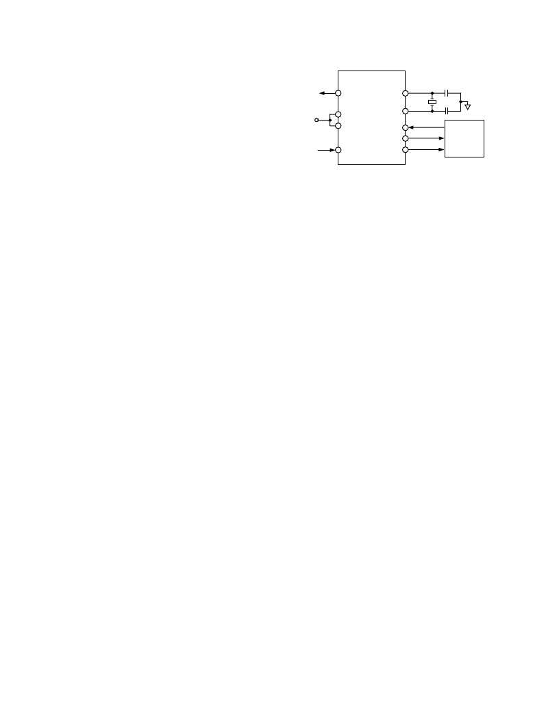
V
DD
CLKOUT
MMAP
BMODE
RESET
XTAL
CLKIN
DR1A
SCLK1
RFS1/
SROM
SERIAL ROM
OR
E
2
PROM
ADMC401
13MHz
20pF
20pF
DATA
CLK
RESET
Figure 15. Basic System Configuration in Standalone
Mode
If boot loading from an SROM or E
2
PROM is unsuccessful, the
monitor code reconfigures SPORT1 as a UART (setting both
Bit 4 and Bit 5 of the MODECTRL register) and attempts to
receive commands from an external device on this serial port
using the DR1B pin. The monitor now waits for two bytes of
information. These bytes are received asynchronously so that no
clock is needed. The first byte is the autobaud byte and it is
used to calculate the baud rate at which data is being received.
This is known as the autobaud feature. The ADMC401 will
automatically lock onto the baud rate of the external device if
it is sent a byte of 0x70. The maximum baud rate that the
ADMC401 will lock onto is 300
kb/s for a 26 MHz CLKOUT.
The second byte of information received is the header byte that
uniquely identifies to the monitor which type of interface it is
connected to. There are six different interfaces supported on the
ADMC401. These includes:
A UART boot loader such as from a Motorola 68HC11
communicating over its Serial Communications Interface
(SCI) port.
A synchronous slave boot loader (the clock is external).
A synchronous master boot loader (the ADMC401 provides
the clock).
A UART debugger interface such as the
Motion Control
Debugger
from Analog Devices. The monitor then processes
commands received from the debugger over the UART
interface.
A synchronous master debugger interface.
A synchronous slave debugger interface.
Detailed information on these software interfaces can be
found in the “UART Boot Loader Protocol” and “UART
Debugger Protocol” appendices of the ADMC401
Developer’s
Reference Manual
.
Byte-Wide EPROM Boot Mode (MMAP = BMODE = 0)
If both the MMAP and BMODE pins are tied to GND, the
ADMC401 operates in the so-called
EPROM Boot
mode. In this
mode the entire internal program memory, or any portion of it,
can be loaded from an external source using a boot sequence
over the memory interface. To allow boot loading from inexpen-
sive 8-bit wide EPROM devices, the processor loads data one
byte at a time. The boot sequence can also be initiated after
reset by software.
Boot memory is organized into eight pages, each of which is 8k
bytes long. Every fourth byte of a page is an
empty
byte except
for the first one, which contains the page length. Each set of
three bytes between successive empty bytes contains one 24-bit
instruction to be loaded into the internal PM RAM of the DSP.
相关PDF资料 |
PDF描述 |
|---|---|
| ADMC401 | Single-Chip, DSP-Based High Performance Motor Controller |
| ADMC401-ADVEVALKIT | Circular Connector; No. of Contacts:5; Series:MS27497; Body Material:Aluminum; Connecting Termination:Crimp; Connector Shell Size:10; Circular Contact Gender:Pin; Circular Shell Style:Wall Mount Receptacle; Insert Arrangement:10-5 RoHS Compliant: No |
| ADMC401-PB | Single-Chip, DSP-Based High Performance Motor Controller |
| ADMCF340 | DashDSPTM 64-Lead Flash Mixed-Signal DSP with Enhanced Analog Front End |
| ADMCF340BST | DashDSPTM 64-Lead Flash Mixed-Signal DSP with Enhanced Analog Front End |
相关代理商/技术参数 |
参数描述 |
|---|---|
| ADMC401BSTZ | 功能描述:IC DSP 8CH 12BIT MOTCTRL 144LQFP RoHS:是 类别:集成电路 (IC) >> 嵌入式 - DSP(数字式信号处理器) 系列:电机控制 标准包装:2 系列:StarCore 类型:SC140 内核 接口:DSI,以太网,RS-232 时钟速率:400MHz 非易失内存:外部 芯片上RAM:1.436MB 电压 - 输入/输出:3.30V 电压 - 核心:1.20V 工作温度:-40°C ~ 105°C 安装类型:表面贴装 封装/外壳:431-BFBGA,FCBGA 供应商设备封装:431-FCPBGA(20x20) 包装:托盘 |
| ADMC401BSTZKL1 | 制造商:Analog Devices 功能描述: |
| ADMC401-PB | 制造商:AD 制造商全称:Analog Devices 功能描述:Single-Chip, DSP-Based High Performance Motor Controller |
| ADMCF326 | 制造商:AD 制造商全称:Analog Devices 功能描述:28-Lead Flash Memory DSP Motor Controller |
| ADMCF326BN | 制造商:Analog Devices 功能描述: |
发布紧急采购,3分钟左右您将得到回复。