- 您现在的位置:买卖IC网 > PDF目录165354 > ADS8517IPWR (TEXAS INSTRUMENTS INC) 1-CH 16-BIT SUCCESSIVE APPROXIMATION ADC, SERIAL/PARALLEL ACCESS, PDSO28 PDF资料下载
参数资料
| 型号: | ADS8517IPWR |
| 厂商: | TEXAS INSTRUMENTS INC |
| 元件分类: | ADC |
| 英文描述: | 1-CH 16-BIT SUCCESSIVE APPROXIMATION ADC, SERIAL/PARALLEL ACCESS, PDSO28 |
| 封装: | GREEN, PLASTIC, TSSOP-28 |
| 文件页数: | 1/38页 |
| 文件大小: | 948K |
| 代理商: | ADS8517IPWR |
当前第1页第2页第3页第4页第5页第6页第7页第8页第9页第10页第11页第12页第13页第14页第15页第16页第17页第18页第19页第20页第21页第22页第23页第24页第25页第26页第27页第28页第29页第30页第31页第32页第33页第34页第35页第36页第37页第38页
ADS8517
ADS8517
1
FEATURES
APPLICATIONS
DESCRIPTION
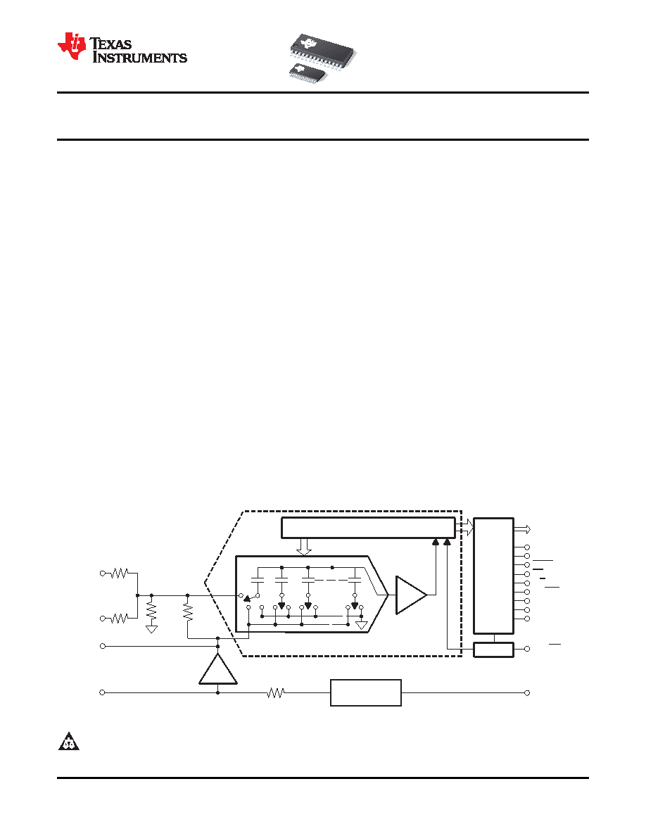
SuccessiveApproximationRegister(SAR)
Comparator
CDAC
Ref
Buffer
BUF
ADC
REF
REF
CAP
R1
IN
40kW
20kW
2.5-V
InternalReference
6kW
Parallel
and
Serial
DataOut
and
Control
Clock
40kW
10kW
R2
IN
REFD
Parallel
Data
PWRD
BYTE
BUSY
CS
R/C
SB/BTC
TAG
SDATA
DATACLK
EXT/INT
www.ti.com ................................................................................................................................................. SLAS527A – SEPTEMBER 2008 – REVISED JUNE 2009
16-Bit, 200-kSPS, Low-Power, Sampling ANALOG-TO-DIGITAL CONVERTER
with Internal Reference and Parallel/Serial Interface
Portable Test Equipment
23
200-kHz Minimum Sampling Rate
USB Data Acquisition Module
4-V, 5-V, and ±10-V Input Ranges with
Medical Equipment
High-Impedance Input
Industrial Process Control
±1.5 LSB Max INL
Digital Signal Processing
+1.5/–1 LSB Max/Min DNL, 16 Bits NMC
Instrumentation
±2-mV Max BPZ, ±0.6 ppm/°C BPZ Drift
±2-mV Max UPZ, ±0.15 ppm/°C UPZ Drift
88.8-dB SINAD with 10-kHz Input
The ADS8517 is a complete low-power, single 5-V
SPI-Compatible Serial Output With
supply,
16-bit
sampling
analog-to-digital
(A/D)
Daisy-Chain (TAG), SPI Master/Slave Feature
converter.
It
contains
a
complete,
16-bit,
Full Parallel Interface
capacitor-based, successive approximation register
(SAR) A/D converter with sample-and-hold, clock,
Binary Twos Complement or Straight Binary
reference, and data interface. The converter can be
Output Code Formats
configured for a variety of input ranges including
Single 4.5-V to 5.5-V Analog Supply, 1.65-V to
±10 V, 4 V, and 5 V. For most input ranges, the input
5.5-V Interface Supply
voltage can swing to 25 V or –25 V without damage
to the device.
Uses Internal 2.5-V or External Reference
No External Precision Resistors Required
An SPI-compatible serial interface allows data to be
synchronized to an internal or external clock. A full
Low Power Dissipation (ADC+REF+BUF):
parallel interface using the selectable BYTE pin is
–
47 mW Typ, 60 mW Max at 200 kSPS
also provided to allow the maximum system design
50-W Max Power-Down Mode
flexibility. The ADS8517 is specified at a 200-kHz
sampling rate over the industrial –40°C to +85°C
Pin-Compatible with 16-Bit ADS7807 and
temperature range.
SO-28 and TSSOP-28 Packages
1
Please be aware that an important notice concerning availability, standard warranty, and use in critical applications of Texas
Instruments semiconductor products and disclaimers thereto appears at the end of this data sheet.
2
SPI is a trademark of Motorola, Inc.
3
All other trademarks are the property of their respective owners.
PRODUCTION DATA information is current as of publication date.
Copyright 2008–2009, Texas Instruments Incorporated
Products conform to specifications per the terms of the Texas
Instruments standard warranty. Production processing does not
necessarily include testing of all parameters.
相关PDF资料 |
PDF描述 |
|---|---|
| ADS8519IRHBR | 3-CH 16-BIT SUCCESSIVE APPROXIMATION ADC, SERIAL ACCESS, PQCC32 |
| ADSP-21060LCWZ-160 | 48-BIT, 40 MHz, OTHER DSP, CQFP240 |
| ADSP-TS101SKB2250X | 64-BIT, 125 MHz, OTHER DSP, PBGA484 |
| ADT70GR-REEL7 | ANALOG TEMP SENSOR-VOLTAGE, 2.49-2.51V, 1Cel, RECTANGULAR, SURFACE MOUNT |
| ADT7462ACPZ-500RL7 | DIGITAL TEMP SENSOR-SERIAL, 8BIT(s), 4Cel, SQUARE, SURFACE MOUNT |
相关代理商/技术参数 |
参数描述 |
|---|---|
| ADS8517W | 制造商:TI 制造商全称:Texas Instruments 功能描述:16-Bit, 200-kSPS, Low-Power, Sampling ANALOG-TO-DIGITAL CONVERTER with Internal Reference and Parallel/Serial Interface |
| ADS8519 | 制造商:TI 制造商全称:Texas Instruments 功能描述:16-BIT 250-KSPS SERIAL CMOS SAMPLING ANALOG-TO-DIGITAL CONVERTER |
| ADS8519_08 | 制造商:TI 制造商全称:Texas Instruments 功能描述:16-Bit, 250kSPS, Serial, CMOS, Sampling ANALOG-TO-DIGITAL CONVERTER |
| ADS8519EVM | 功能描述:数据转换 IC 开发工具 ADS8519 Eval Mod RoHS:否 制造商:Texas Instruments 产品:Demonstration Kits 类型:ADC 工具用于评估:ADS130E08 接口类型:SPI 工作电源电压:- 6 V to + 6 V |
| ADS8519I | 制造商:TI 制造商全称:Texas Instruments 功能描述:16-Bit, 250kSPS, Serial, CMOS, Sampling ANALOG-TO-DIGITAL CONVERTER |
发布紧急采购,3分钟左右您将得到回复。