- 您现在的位置:买卖IC网 > PDF目录20610 > ISL6613IRZ-T (Intersil)IC MOSFET DRVR SYNC BUCK 10-DFN PDF资料下载
参数资料
| 型号: | ISL6613IRZ-T |
| 厂商: | Intersil |
| 文件页数: | 5/12页 |
| 文件大小: | 0K |
| 描述: | IC MOSFET DRVR SYNC BUCK 10-DFN |
| 标准包装: | 6,000 |
| 配置: | 高端和低端,同步 |
| 输入类型: | PWM |
| 延迟时间: | 10ns |
| 电流 - 峰: | 1.25A |
| 配置数: | 1 |
| 输出数: | 2 |
| 高端电压 - 最大(自引导启动): | 36V |
| 电源电压: | 10.8 V ~ 13.2 V |
| 工作温度: | -40°C ~ 85°C |
| 安装类型: | 表面贴装 |
| 封装/外壳: | 10-VFDFN 裸露焊盘 |
| 供应商设备封装: | 10-DFN(3x3) |
| 包装: | 带卷 (TR) |
�� �
�
�ISL6612,� ISL6613�
�Absolute� Maximum� Ratings�
�Supply� Voltage� (VCC)� .� .� .� .� .� .� .� .� .� .� .� .� .� .� .� .� .� .� .� .� .� .� .� .� .� .� .� .� .� .� .� .� .15V�
�Supply� Voltage� (PVCC)� .� .� .� .� .� .� .� .� .� .� .� .� .� .� .� .� .� .� .� .� .� .� .� .� .� VCC� +� 0.3V�
�Input� Voltage� (V� PWM� )� .� .� .� .� .� .� .� .� .� .� .� .� .� .� .� .� .� .� .� .� .� .� GND� -� 0.3V� to� 7V�
�BOOT� Voltage� (V� BOOT-GND� ).� .� .� .� .� .� .� .� .� .� .� .� .� .� .� .� .� .� .� .� .� .� .� .� .� .� .� .36V�
�BOOT� To� PHASE� Voltage� (V� BOOT-PHASE� )� .� .� .� .� .� -0.3V� to� 15V� (DC)�
�.� .� .� .� .� .� .� .� .� .� .� .� .� .� .� .� .� .� .� .� .� .� .� .� .� .� .� .� .� .� .� .� -0.3V� to� 16V� (<10ns,� 10μJ)�
�UGATE.� .� .� .� .� .� .� .� .� .� .� .� .� .� .� .� .� .� .� V� PHASE� -� 0.3V� DC� to� V� BOOT� +� 0.3V�
�V� PHASE� -� 3.5V� (<100ns� Pulse� Width,� 2μJ)� to� V� BOOT� +� 0.3V�
�LGATE� .� .� .� .� .� .� .� .� .� .� .� .� .� .� .� .� .� .� .� .� .� .� GND� -� 0.3V� DC� to� V� PVCC� +� 0.3V�
�GND� -� 5V� (<100ns� Pulse� Width,� 2μJ)� to� V� PVCC� +� 0.3V�
�PHASE.� .� .� .� .� .� .� .� .� .� .� .� .� .� .� .� .� .� .� .� .� .� .� .� .� .� .� .GND� -� 0.3VDC� to� 24VDC�
�GND� -� 8V� (<400ns,� 20μJ)� to� 31V� (<200ns,� V� BOOT-GND� <� 36V)�
�ESD� Rating�
�Human� Body� Model� .� .� .� .� .� .� .� .� .� .� .� .� .� .� .� .� .� .� .� .� Class� I� JEDEC� STD�
�Thermal� Information�
�Thermal� Resistance� θ� JA� (°C/W)� θ� JC� (°C/W)�
�8� Ld� SOIC� Package� (Note� 4)� .� .� .� .� .� .� .� .� 100� N/A�
�8� Ld� EPSOIC� Package� (Notes� 5,� 6).� .� .� 50� 7�
�10� Ld� DFN� Package� (Notes� 5,� 6)� .� .� .� .� .� 48� 7�
�Maximum� Junction� Temperature� (Plastic� Package)� .� .� .� .� .� .� .� +150°C�
�Maximum� Storage� Temperature� Range� .� .� .� .� .� .� .� .� .� .-65°C� to� +150°C�
�Pb-Free� Reflow� Profile.� .� .� .� .� .� .� .� .� .� .� .� .� .� .� .� .� .� .� .� .� .� .� .� .see� link� below�
�http://www.intersil.com/pbfree/Pb-FreeReflow.asp�
�Recommended� Operating� Conditions�
�Ambient� Temperature� Range.� .� .� .� .� .� .� .� .� .� .� .� .� .� .� .� .� .� .-40°C� to� +85°C�
�Maximum� Operating� Junction� Temperature.� .� .� .� .� .� .� .� .� .� .� .� .� +125°C�
�Supply� Voltage,� VCC� .� .� .� .� .� .� .� .� .� .� .� .� .� .� .� .� .� .� .� .� .� .� .� .� .� .� .� .� .12V� ±� 10%�
�Supply� Voltage� Range,� PVCC� .� .� .� .� .� .� .� .� .� .� .� .� .� .� .� .� 5V� to� 12V� ±� 10%�
�CAUTION:� Do� not� operate� at� or� near� the� maximum� ratings� listed� for� extended� periods� of� time.� Exposure� to� such� conditions� may� adversely� impact� product� reliability� and�
�result� in� failures� not� covered� by� warranty.�
�NOTES:�
�4.� θ� JA� is� measured� with� the� component� mounted� on� a� high� effective� thermal� conductivity� test� board� in� free� air.�
�5.� θ� JA� is� measured� in� free� air� with� the� component� mounted� on� a� high� effective� thermal� conductivity� test� board� with� “direct� attach”� features.� See�
�Tech� Brief� TB379.�
�6.� For� θ� JC� ,� the� “case� temp”� location� is� the� center� of� the� exposed� metal� pad� on� the� package� underside.�
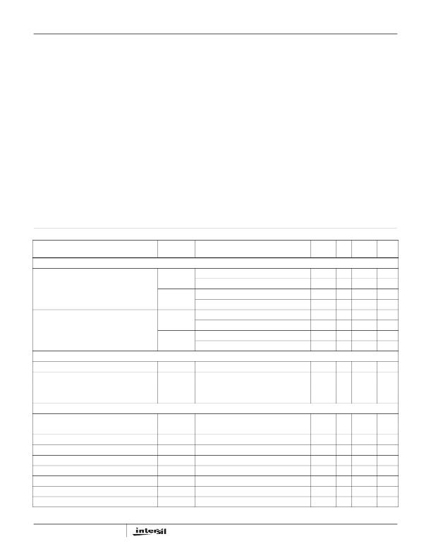
�Electrical� Specifications�
�Recommended� Operating� Conditions,� Unless� Otherwise� Noted.�
�MIN�
�MAX�
�PARAMETER�
�SYMBOL�
�TEST� CONDITIONS�
�(Note� 8)� TYP� (Note� 8)� UNITS�
�VCC� SUPPLY� CURRENT�
�Bias� Supply� Current�
�Gate� Drive� Bias� Current�
�I� VCC�
�I� VCC�
�I� PVCC�
�I� PVCC�
�ISL6612,� f� PWM� =� 300kHz,� V� VCC� =� 12V�
�ISL6613,� f� PWM� =� 300kHz,� V� VCC� =� 12V�
�ISL6612,� f� PWM� =� 1MHz,� V� VCC� =� 12V�
�ISL6613,� f� PWM� =� 1MHz,� V� VCC� =� 12V�
�ISL6612,� f� PWM� =� 300kHz,� V� PVCC� =� 12V�
�ISL6613,� f� PWM� =� 300kHz,� V� PVCC� =� 12V�
�ISL6612,� f� PWM� =� 1MHz,� V� PVCC� =� 12V�
�ISL6613,� f� PWM� =� 1MHz,� V� PVCC� =� 12V�
�-�
�-�
�-�
�-�
�-�
�-�
�-�
�-�
�7.2�
�4.5�
�11�
�5�
�2.5�
�5.2�
�7�
�13�
�-�
�-�
�-�
�-�
�-�
�-�
�-�
�-�
�mA�
�mA�
�mA�
�mA�
�mA�
�mA�
�mA�
�mA�
�POWER-ON� RESET� AND� ENABLE�
�VCC� Rising� Threshold�
�VCC� Rising� Threshold�
�VCC� Falling� Threshold�
�VCC� Falling� Threshold�
�T� A� =� 0°C� to� +85°C�
�T� A� =� -40°C� to� +85°C�
�T� A� =� 0°C� to� +85°C�
�T� A� =� -40°C� to� +85°C�
�9.35�
�8.35�
�7.35�
�6.35�
�9.80�
�9.80�
�7.60�
�7.60�
�10.00�
�10.00�
�8.00�
�8.00�
�V�
�V�
�V�
�V�
�PWM� INPUT� (See� “TIMING� DIAGRAM”� on� page� 7)�
�Input� Current�
�PWM� Rising� Threshold�
�PWM� Falling� Threshold�
�Typical� Three-State� Shutdown� Window�
�Three-State� Lower� Gate� Falling� Threshold�
�Three-State� Lower� Gate� Rising� Threshold�
�Three-State� Upper� Gate� Rising� Threshold�
�Three-State� Upper� Gate� Falling� Threshold�
�I� PWM�
�V� PWM� =� 5V�
�V� PWM� =� 0V�
�VCC� =� 12V�
�VCC� =� 12V�
�VCC� =� 12V�
�VCC� =� 12V�
�VCC� =� 12V�
�VCC� =� 12V�
�VCC� =� 12V�
�-�
�-�
�-�
�-�
�1.80�
�-�
�-�
�-�
�-�
�450�
�-400�
�3.00�
�2.00�
�1.50�
�1.00�
�3.20�
�2.60�
�-�
�-�
�-�
�-�
�2.40�
�-�
�-�
�-�
�-�
�μA�
�μA�
�V�
�V�
�V�
�V�
�V�
�V�
�V�
�5�
�FN9153.9�
�June� 15,� 2010�
�相关PDF资料 |
PDF描述 |
|---|---|
| V48C28H75B3 | CONVERTER MOD DC/DC 28V 75W |
| 78M6612-GT/F/P2 | IC PWR MEASUREMENT AC 64LQFP |
| SLF6045T-150M1R3-3PF | INDUCTOR POWER 15UH 1.3A SMD |
| LXV150-024SW | POWER SUPPLY LED IP67 150W 24V |
| LM4040C30IDCKR | IC VREF SHUNT PREC 3V SC-70-5 |
相关代理商/技术参数 |
参数描述 |
|---|---|
| ADV7511WBSWZ-RL | 功能描述:IC XMITTER HDMI AUTO 64LQFP RoHS:是 类别:集成电路 (IC) >> 接口 - 驱动器,接收器,收发器 系列:- 标准包装:27 系列:- 类型:收发器 驱动器/接收器数:3/3 规程:RS232,RS485 电源电压:4.75 V ~ 5.25 V 安装类型:表面贴装 封装/外壳:28-SOIC(0.295",7.50mm 宽) 供应商设备封装:28-SOIC 包装:管件 |
| ADV7513 | 制造商:AD 制造商全称:Analog Devices 功能描述:165 MHz, High Performance |
| ADV7513BSWZ | 功能描述:IC TX HDMI 165MHZ 64LQFP RoHS:是 类别:集成电路 (IC) >> 线性 - 视频处理 系列:- 标准包装:250 系列:- 类型:电平移位器 应用:LCD 电视机/监控器 安装类型:表面贴装 封装/外壳:28-WFQFN 裸露焊盘 供应商设备封装:28-WQFN(4x4)裸露焊盘 包装:带卷 (TR) 其它名称:296-32523-2TPS65198RUYT-ND |
| ADV7520 | 制造商:AD 制造商全称:Analog Devices 功能描述:Low Power HDMI/DVI Transmitter with Consumer Electronic Control (CEC) |
| ADV7520/PCBZ | 制造商:AD 制造商全称:Analog Devices 功能描述:Low Power HDMI/DVI Transmitter with Consumer Electronic Control (CEC) |
发布紧急采购,3分钟左右您将得到回复。