- 您现在的位置:买卖IC网 > PDF目录20610 > ISL6613IRZ-T (Intersil)IC MOSFET DRVR SYNC BUCK 10-DFN PDF资料下载
参数资料
| 型号: | ISL6613IRZ-T |
| 厂商: | Intersil |
| 文件页数: | 9/12页 |
| 文件大小: | 0K |
| 描述: | IC MOSFET DRVR SYNC BUCK 10-DFN |
| 标准包装: | 6,000 |
| 配置: | 高端和低端,同步 |
| 输入类型: | PWM |
| 延迟时间: | 10ns |
| 电流 - 峰: | 1.25A |
| 配置数: | 1 |
| 输出数: | 2 |
| 高端电压 - 最大(自引导启动): | 36V |
| 电源电压: | 10.8 V ~ 13.2 V |
| 工作温度: | -40°C ~ 85°C |
| 安装类型: | 表面贴装 |
| 封装/外壳: | 10-VFDFN 裸露焊盘 |
| 供应商设备封装: | 10-DFN(3x3) |
| 包装: | 带卷 (TR) |
�� �
�
�ISL6612,� ISL6613�
�is� approximately� 800mW� at� room� temperature,� while� the�
�power� dissipation� capacity� in� the� EPSOIC� and� DFN�
�packages,� with� an� exposed� heat� escape� pad,� is� more� than� 2W�
�and� 1.5W,� respectively.� Both� EPSOIC� and� DFN� packages� are�
�UVCC�
�BOOT�
�C� GD�
�D�
�more� suitable� for� high� frequency� applications.� See� “Layout�
�Considerations”� on� page� 9� for� thermal� transfer� improvement�
�suggestions.� When� designing� the� driver� into� an� application,� it�
�is� recommended� that� the� following� calculation� is� used� to�
�ensure� safe� operation� at� the� desired� frequency� for� the�
�R� HI1�
�R� LO1�
�G�
�R� G1�
�R� GI1�
�C� GS�
�S�
�C� DS�
�Q� 1�
�selected� MOSFETs.� The� total� gate� drive� power� losses� due� to�
�the� gate� charge� of� MOSFETs� and� the� driver’s� internal� circuitry�
�and� their� corresponding� average� driver� current� can� be�
�estimated� using� Equation� 2� and� Equation� 3,� respectively,�
�PHASE�
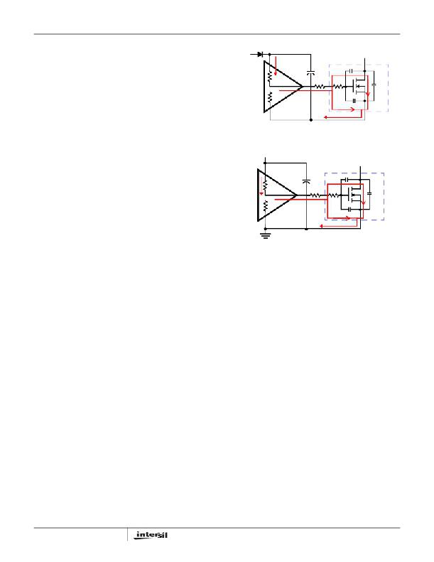
�FIGURE� 3.� TYPICAL� UPPER-GATE� DRIVE� TURN-ON� PATH�
�P� Qg_TOT� =� P� Qg_Q1� +� P� Qg_Q2� +� I� Q� ?� VCC�
�(EQ.� 2)�
�LVCC�
�D�
�Q� G1� ?� UVCC� 2�
�P� Qg_Q1� =� ---------------------------------------� ?� F� SW� ?� N� Q1�
�Q� G2�
�P� Qg_Q2� =� --------------------------------------� ?� F� SW� ?� N� Q2�
�V� GS1�
�?� LVCC� 2�
�V� GS2�
�R� HI2�
�R� LO2�
�G�
�R� G2�
�C� GD�
�R� GI2�
�C� GS�
�C� DS�
�Q� 2�
�?� Q� G1� ?� UVCC� ?� N� Q1� Q� G2� ?� LVCC� ?� N� Q2� ?�
�I� DR� =� ?� ------------------------------------------------------� +� -----------------------------------------------------� ?� ?� F� SW� +� I� Q�
�P� DR_UP� =� ?� --------------------------------------� +� ----------------------------------------� ?� ?� ---------------------�
�R� HI1� +� R� EXT1� R� LO1� +� R� EXT1� ?�
�?�
�P� DR_LOW� =� ?� --------------------------------------� +� ----------------------------------------� ?� ?� ---------------------�
�?� R� HI2� +� R� EXT2� R� LO2� +� R� EXT2� ?�
�?� V� GS1� V� GS2� ?�
�(EQ.� 3)�
�where� the� gate� charge� (Q� G1� and� Q� G2� )� is� defined� at� a�
�particular� gate� to� source� voltage� (V� GS1� and� V� GS2� )� in� the�
�corresponding� MOSFET� data� sheet;� I� Q� is� the� driver� ’s� total�
�quiescent� current� with� no� load� at� both� drive� outputs;� N� Q1�
�and� N� Q2� are� number� of� upper� and� lower� MOSFETs,�
�respectively;� UVCC� and� LVCC� are� the� drive� voltages� for�
�both� upper� and� lower� FETs,� respectively.� The� I� Q*� VCC�
�product� is� the� quiescent� power� of� the� driver� without�
�capacitive� load� and� is� typically� 116mW� at� 300kHz.�
�The� total� gate� drive� power� losses� are� dissipated� among� the�
�resistive� components� along� the� transition� path.� The� drive�
�resistance� dissipates� a� portion� of� the� total� gate� drive� power�
�losses,� the� rest� will� be� dissipated� by� the� external� gate�
�resistors� (R� G1� and� R� G2� )� and� the� internal� gate� resistors� (R� GI1�
�and� R� GI2� )� of� MOSFETs.� Figures� 3� and� 4� show� the� typical�
�upper� and� lower� gate� drives� turn-on� transition� path.� The�
�power� dissipation� on� the� driver� can� be� roughly� estimated� as:�
�P� DR� =� P� DR_UP� +� P� DR_LOW� +� I� Q� ?� VCC�
�?� R� HI1� R� LO1� ?� P� Qg_Q1�
�2�
�?� R� HI2� R� LO2� ?� P� Qg_Q2�
�2�
�S�
�FIGURE� 4.� TYPICAL� LOWER-GATE� DRIVE� TURN-ON� PATH�
�Layout� Considerations�
�For� heat� spreading,� place� copper� underneath� the� IC� whether�
�it� has� an� exposed� pad� or� not.� The� copper� area� can� be�
�extended� beyond� the� bottom� area� of� the� IC� and/or�
�connected� to� buried� copper� plane(s)� with� thermal� vias.� This�
�combination� of� vias� for� vertical� heat� escape,� extended�
�copper� plane,� and� buried� planes� for� heat� spreading� allows�
�the� IC� to� achieve� its� full� thermal� potential.�
�Place� each� channel� power� component� as� close� to� each�
�other� as� possible� to� reduce� PCB� copper� losses� and� PCB�
�parasitics:� shortest� distance� between� DRAINs� of� upper� FETs�
�and� SOURCEs� of� lower� FETs;� shortest� distance� between�
�DRAINs� of� lower� FETs� and� the� power� ground.� Thus,� smaller�
�amplitudes� of� positive� and� negative� ringing� are� on� the�
�switching� edges� of� the� PHASE� node.� However,� some� space�
�in� between� the� power� components� is� required� for� good�
�airflow.� The� traces� from� the� drivers� to� the� FETs� should� be�
�kept� short� and� wide� to� reduce� the� inductance� of� the� traces�
�and� to� promote� clean� drive� signals.�
�N�
�R� GI1�
�R� EXT1� =� R� G1� +� -------------�
�Q1�
�N�
�R� GI2�
�R� EXT2� =� R� G2� +� -------------�
�Q2�
�(EQ.� 4)�
�9�
�FN9153.9�
�June� 15,� 2010�
�相关PDF资料 |
PDF描述 |
|---|---|
| V48C28H75B3 | CONVERTER MOD DC/DC 28V 75W |
| 78M6612-GT/F/P2 | IC PWR MEASUREMENT AC 64LQFP |
| SLF6045T-150M1R3-3PF | INDUCTOR POWER 15UH 1.3A SMD |
| LXV150-024SW | POWER SUPPLY LED IP67 150W 24V |
| LM4040C30IDCKR | IC VREF SHUNT PREC 3V SC-70-5 |
相关代理商/技术参数 |
参数描述 |
|---|---|
| ADV7511WBSWZ-RL | 功能描述:IC XMITTER HDMI AUTO 64LQFP RoHS:是 类别:集成电路 (IC) >> 接口 - 驱动器,接收器,收发器 系列:- 标准包装:27 系列:- 类型:收发器 驱动器/接收器数:3/3 规程:RS232,RS485 电源电压:4.75 V ~ 5.25 V 安装类型:表面贴装 封装/外壳:28-SOIC(0.295",7.50mm 宽) 供应商设备封装:28-SOIC 包装:管件 |
| ADV7513 | 制造商:AD 制造商全称:Analog Devices 功能描述:165 MHz, High Performance |
| ADV7513BSWZ | 功能描述:IC TX HDMI 165MHZ 64LQFP RoHS:是 类别:集成电路 (IC) >> 线性 - 视频处理 系列:- 标准包装:250 系列:- 类型:电平移位器 应用:LCD 电视机/监控器 安装类型:表面贴装 封装/外壳:28-WFQFN 裸露焊盘 供应商设备封装:28-WQFN(4x4)裸露焊盘 包装:带卷 (TR) 其它名称:296-32523-2TPS65198RUYT-ND |
| ADV7520 | 制造商:AD 制造商全称:Analog Devices 功能描述:Low Power HDMI/DVI Transmitter with Consumer Electronic Control (CEC) |
| ADV7520/PCBZ | 制造商:AD 制造商全称:Analog Devices 功能描述:Low Power HDMI/DVI Transmitter with Consumer Electronic Control (CEC) |
发布紧急采购,3分钟左右您将得到回复。