- 您现在的位置:买卖IC网 > PDF目录381345 > AS7C3364FT32B-80TQCN (ALLIANCE SEMICONDUCTOR CORP) 3.3V 64K x 32/36 Flow Through Synchronous SRAM PDF资料下载
参数资料
| 型号: | AS7C3364FT32B-80TQCN |
| 厂商: | ALLIANCE SEMICONDUCTOR CORP |
| 元件分类: | DRAM |
| 英文描述: | 3.3V 64K x 32/36 Flow Through Synchronous SRAM |
| 中文描述: | 64K X 32 STANDARD SRAM, 8 ns, PQFP100 |
| 封装: | 14 X 20 MM, LEAD FREE, TQFP-100 |
| 文件页数: | 5/19页 |
| 文件大小: | 417K |
| 代理商: | AS7C3364FT32B-80TQCN |
AS7C3364FT32B
AS7C3364FT36B
2/8/05; v.1.2
Alliance Semiconductor
P. 5 of 19
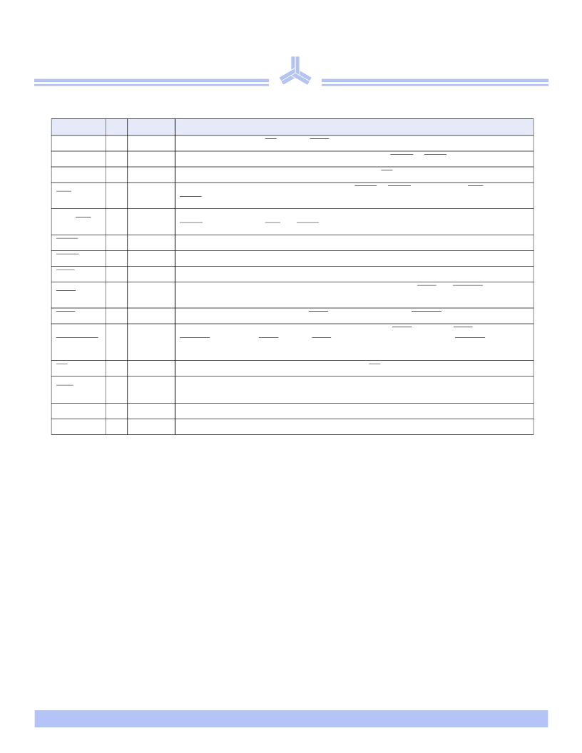
Signal descriptions
Snooze Mode
SNOOZE MODE is a low current, power-down mode in which the device is deselected and current is reduced to I
SB2
. The duration of
SNOOZE MODE is dictated by the length of time the ZZ is in a High state.
The ZZ pin is an asynchronous, active high input that causes the device to enter SNOOZE MODE.
When the ZZ pin becomes a logic High, I
SB2
is guaranteed after the time t
ZZI
is met. After entering SNOOZE MODE, all inputs except ZZ
is disabled and all outputs go to High-Z. Any operation pending when entering SNOOZE MODE is not guaranteed to successfully complete.
Therefore, SNOOZE MODE (READ or WRITE) must not be initiated until valid pending operations are completed. Similarly, when exiting
SNOOZE MODE during t
PUS
, only a DESELECT or READ cycle should be given while the SRAM is transitioning out of SNOOZE MODE.
Pin
I/O
Properties
Description
CLK
I
CLOCK
Clock. All inputs except OE, ZZ, and LBO are synchronous to this clock.
A,A0,A1
I
SYNC
Address. Sampled when all chip enables are active and when ADSC or ADSP are asserted.
DQ[a,b,c,d]
I/O
SYNC
Data. Driven as output when the chip is enabled and when OE is active.
CE0
I
SYNC
Master chip enable. Sampled on clock edges when ADSP or ADSC is active. When CE0 is inactive,
ADSP is blocked. Refer to the “Synchronous truth table” for more information.
CE1, CE2
I
SYNC
Synchronous chip enables, active high, and active low, respectively. Sampled on clock edges when
ADSC is active or when CE0 and ADSP are active.
ADSP
I
SYNC
Address strobe processor. Asserted low to load a new address or to enter standby mode.
ADSC
I
SYNC
Address strobe controller. Asserted low to load a new address or to enter standby mode.
ADV
I
SYNC
Advance. Asserted low to continue burst read/write.
GWE
I
SYNC
Global write enable. Asserted low to write all 32/36 bits. When high, BWE and BW[a:d] control write
enable.
BWE
I
SYNC
Byte write enable. Asserted low with GWE high to enable effect of BW[a:d] inputs.
BW[a,b,c,d]
I
SYNC
Write enables. Used to control write of individual bytes when GWE is high and BWE is low. If any of
BW[a:d] is active with GWE high and BWE low, the cycle is a write cycle. If all BW[a:d] are inactive,
the cycle is a read cycle.
OE
I
ASYNC
Asynchronous output enable. I/O pins are driven when OE is active and chip is in read mode.
LBO
I
STATIC
Selects Burst mode. When tied to V
DD
or left floating, device follows interleaved Burst order. When
driven Low, device follows linear Burst order.
This signal is internally pulled High.
ZZ
I
ASYNC
Snooze. Places device in low power mode; data is retained. Connect to GND if unused.
NC
-
-
No connect
相关PDF资料 |
PDF描述 |
|---|---|
| AS7C3364FT32B-80TQI | 3.3V 64K x 32/36 Flow Through Synchronous SRAM |
| AS7C3364FT32B-80TQIN | 3.3V 64K x 32/36 Flow Through Synchronous SRAM |
| AS7C3364FT36B-10TQCN | 3.3V 64K x 32/36 Flow Through Synchronous SRAM |
| AS7C3364FT36B-10TQI | 3.3V 64K x 32/36 Flow Through Synchronous SRAM |
| AS7C3364FT36B-10TQIN | 3.3V 64K x 32/36 Flow Through Synchronous SRAM |
相关代理商/技术参数 |
参数描述 |
|---|---|
| AS7C3364FT32B-80TQI | 制造商:ALSC 制造商全称:Alliance Semiconductor Corporation 功能描述:3.3V 64K x 32/36 Flow Through Synchronous SRAM |
| AS7C3364FT32B-80TQIN | 制造商:ALSC 制造商全称:Alliance Semiconductor Corporation 功能描述:3.3V 64K x 32/36 Flow Through Synchronous SRAM |
| AS7C3364FT36B-10TQC | 制造商:ALSC 制造商全称:Alliance Semiconductor Corporation 功能描述:3.3V 64K x 32/36 Flow Through Synchronous SRAM |
| AS7C3364FT36B-10TQCN | 制造商:ALSC 制造商全称:Alliance Semiconductor Corporation 功能描述:3.3V 64K x 32/36 Flow Through Synchronous SRAM |
| AS7C3364FT36B-10TQI | 制造商:ALSC 制造商全称:Alliance Semiconductor Corporation 功能描述:3.3V 64K x 32/36 Flow Through Synchronous SRAM |
发布紧急采购,3分钟左右您将得到回复。