参数资料
| 型号: | X40020V14-A |
| 厂商: | Intersil |
| 文件页数: | 11/24页 |
| 文件大小: | 0K |
| 描述: | IC VOLTAGE MONITOR DUAL 14-TSSOP |
| 标准包装: | 95 |
| 类型: | 多压监控器 |
| 监视电压数目: | 2 |
| 输出: | 开路漏极或开路集电极 |
| 复位: | 高有效 |
| 复位超时: | 可调节/可选择 |
| 电压 - 阀值: | 2.9V,4.6V |
| 工作温度: | 0°C ~ 70°C |
| 安装类型: | 表面贴装 |
| 封装/外壳: | 14-TSSOP(0.173",4.40mm 宽) |
| 供应商设备封装: | 14-TSSOP |
| 包装: | 管件 |
�� �
�
�X40020,� 40021�
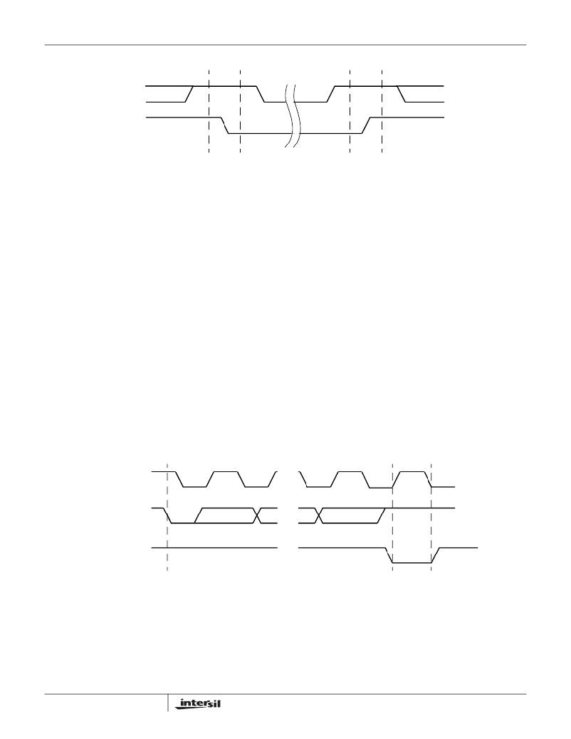
�Figure� 8.� Valid� Start� and� Stop� Conditions�
�SCL�
�SDA�
�Start�
�Serial� Acknowledge�
�Acknowledge� is� a� software� convention� used� to� indi-�
�cate� successful� data� transfer.� The� transmitting� device,�
�either� master� or� slave,� will� release� the� bus� after� trans-�
�mitting� eight� bits.� During� the� ninth� clock� cycle,� the�
�receiver� will� pull� the� SDA� line� LOW� to� acknowledge�
�that� it� received� the� eight� bits� of� data.� See� Figure� 9.�
�The� device� will� respond� with� an� acknowledge� after�
�recognition� of� a� start� condition� and� if� the� correct�
�Device� Identifier� and� Select� bits� are� contained� in� the�
�Slave� Address� Byte.� If� a� write� operation� is� selected,�
�the� device� will� respond� with� an� acknowledge� after� the�
�receipt� of� each� subsequent� eight� bit� word.� The� device�
�will� acknowledge� all� incoming� data� and� address� bytes,�
�except� for� the� Slave� Address� Byte� when� the� Device�
�Identifier� and/or� Select� bits� are� incorrect.�
�In� the� read� mode,� the� device� will� transmit� eight� bits� of�
�data,� release� the� SDA� line,� then� monitor� the� line� for� an�
�acknowledge.� If� an� acknowledge� is� detected� and� no�
�stop� condition� is� generated� by� the� master,� the� device�
�will� continue� to� transmit� data.� The� device� will� terminate�
�further� data� transmissions� if� an� acknowledge� is� not�
�Figure� 9.� Acknowledge� Response� From� Receiver�
�Stop�
�detected.� The� master� must� then� issue� a� stop� condition�
�to� return� the� device� to� Standby� mode� and� place� the�
�device� into� a� known� state.�
�Serial� Write� Operations�
�Byte� Write�
�For� a� write� operation,� the� device� requires� the� Slave�
�Address� Byte� and� a� Word� Address� Byte.� This� gives�
�the� master� access� to� any� one� of� the� words� in� the�
�array.� After� receipt� of� the� Word� Address� Byte,� the�
�device� responds� with� an� acknowledge,� and� awaits� the�
�next� eight� bits� of� data.� After� receiving� the� 8� bits� of� the�
�Data� Byte,� the� device� again� responds� with� an�
�acknowledge.� The� master� then� terminates� the� transfer�
�by� generating� a� stop� condition,� at� which� time� the�
�device� begins� the� internal� write� cycle� to� the� nonvolatile�
�memory.� During� this� internal� write� cycle,� the� device�
�inputs� are� disabled,� so� the� device� will� not� respond� to� any�
�requests� from� the� master.� The� SDA� output� is� at� high�
�impedance.�
�SCL� from�
�Master�
�1�
�8�
�9�
�Data� Output�
�from�
�Data� Output�
�from� Receiver�
�Start�
�11�
�Acknowledge�
�FN8112.1�
�May� 17,� 2006�
�相关PDF资料 |
PDF描述 |
|---|---|
| LD6806CX4/16H,315 | IC REG LDO 1.6V .2A 4WLCSP |
| RCA18DTBT | CONN EDGECARD 36POS R/A .125 SLD |
| 450MXH270MEFCSN30X30 | CAP ALUM 270UF 450V 20% SNAP-IN |
| UWZ1C471MCL1GS | CAP ALUM 470UF 16V 20% SMD |
| 450VXG270MEFCSN25X50 | CAP ALUM 270UF 450V 20% SNAP-IN |
相关代理商/技术参数 |
参数描述 |
|---|---|
| AT91SAM7X256B-CU-999 | 功能描述:ARM微控制器 - MCU IND TEMP MRL B RoHS:否 制造商:STMicroelectronics 核心:ARM Cortex M4F 处理器系列:STM32F373xx 数据总线宽度:32 bit 最大时钟频率:72 MHz 程序存储器大小:256 KB 数据 RAM 大小:32 KB 片上 ADC:Yes 工作电源电压:1.65 V to 3.6 V, 2 V to 3.6 V, 2.2 V to 3.6 V 工作温度范围:- 40 C to + 85 C 封装 / 箱体:LQFP-48 安装风格:SMD/SMT |
| AT91SAM7X256C-AU | 功能描述:微处理器 - MPU LQFP GRN IND TMP MRL C RoHS:否 制造商:Atmel 处理器系列:SAMA5D31 核心:ARM Cortex A5 数据总线宽度:32 bit 最大时钟频率:536 MHz 程序存储器大小:32 KB 数据 RAM 大小:128 KB 接口类型:CAN, Ethernet, LIN, SPI,TWI, UART, USB 工作电源电压:1.8 V to 3.3 V 最大工作温度:+ 85 C 安装风格:SMD/SMT 封装 / 箱体:FBGA-324 |
| AT91SAM7X256C-AUR | 功能描述:ARM微控制器 - MCU LQFP Green IND TEMP MRL B, T&R MRLC RoHS:否 制造商:STMicroelectronics 核心:ARM Cortex M4F 处理器系列:STM32F373xx 数据总线宽度:32 bit 最大时钟频率:72 MHz 程序存储器大小:256 KB 数据 RAM 大小:32 KB 片上 ADC:Yes 工作电源电压:1.65 V to 3.6 V, 2 V to 3.6 V, 2.2 V to 3.6 V 工作温度范围:- 40 C to + 85 C 封装 / 箱体:LQFP-48 安装风格:SMD/SMT |
| AT91SAM7X256C-CU | 功能描述:微处理器 - MPU TFBGA GRN IND TEMP MRL C RoHS:否 制造商:Atmel 处理器系列:SAMA5D31 核心:ARM Cortex A5 数据总线宽度:32 bit 最大时钟频率:536 MHz 程序存储器大小:32 KB 数据 RAM 大小:128 KB 接口类型:CAN, Ethernet, LIN, SPI,TWI, UART, USB 工作电源电压:1.8 V to 3.3 V 最大工作温度:+ 85 C 安装风格:SMD/SMT 封装 / 箱体:FBGA-324 |
| AT91SAM7X256C-CUR | 制造商:Atmel Corporation 功能描述:BGA, GREEN, IND TEMP - Tape and Reel 制造商:Atmel Corporation 功能描述:IC MCU ARM7 256KB FLASH 100TFBGA |
发布紧急采购,3分钟左右您将得到回复。