- 您现在的位置:买卖IC网 > PDF目录379698 > ATT3042-50S132I (Electronic Theatre Controls, Inc.) Field-Programmable Gate Arrays PDF资料下载
参数资料
| 型号: | ATT3042-50S132I |
| 厂商: | Electronic Theatre Controls, Inc. |
| 元件分类: | FPGA |
| 英文描述: | Field-Programmable Gate Arrays |
| 中文描述: | 现场可编程门阵列 |
| 文件页数: | 65/80页 |
| 文件大小: | 528K |
| 代理商: | ATT3042-50S132I |
第1页第2页第3页第4页第5页第6页第7页第8页第9页第10页第11页第12页第13页第14页第15页第16页第17页第18页第19页第20页第21页第22页第23页第24页第25页第26页第27页第28页第29页第30页第31页第32页第33页第34页第35页第36页第37页第38页第39页第40页第41页第42页第43页第44页第45页第46页第47页第48页第49页第50页第51页第52页第53页第54页第55页第56页第57页第58页第59页第60页第61页第62页第63页第64页当前第65页第66页第67页第68页第69页第70页第71页第72页第73页第74页第75页第76页第77页第78页第79页第80页
Data Sheet
February 1997
ATT3000 Series Field-Programmable Gate Arrays
Lucent Technologies Inc.
65
Electrical Characteristics
(continued)
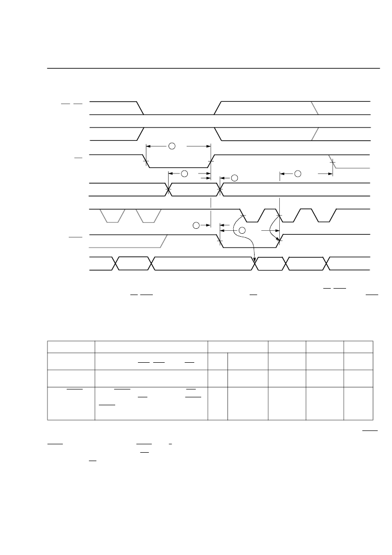
Note: The requirements in this timing diagram are extremely relaxed; data need not be held beyond the rising edge of
WS
.
BUSY
will go active
within 60 ns after the end of
WS
.
BUSY
will stay active for several microseconds.
WS
may be asserted immediately after the end of
BUSY
.
Figure 38. Peripheral Mode Switching Characteristics
Notes:
At powerup, V
CC
must rise from 2.0 V to V
CC
minimum in less than 25 ms. If this is not possible, configuration can be delayed by holding
RESET
low until V
CC
has reached 4.0 V. A very long V
CC
rise time of >100 ms, or a nonmonotonically rising V
CC
may require a >1 μs high level on
RESET
, followed by >6 μs low level on
RESET
and D/
P
after V
CC
has reached 4.0 V.
Configuration must be delayed until the
INIT
of all FPGAs is high.
Time from end of
WS
to CCLK cycle for the new byte of data depends on completion of previous byte processing and the phase of the
internal timing generator for CCLK.
CCLK and DOUT timing is tested in slave mode.
T
BUSY
indicates that the double-buffered parallel-to-serial converter is not yet ready to receive new data. The shortest T
BUSY
occurs when a
byte is loaded into an empty parallel-to-serial converter. The longest T
BUSY
occurs when a new word is loaded into the input register before the
second-level buffer has started shifting out data.
Table 28. Peripheral Mode Switching Characteristics
Signal
Write Signal
Description
Symbol
Min
Max
Unit
Effective Write Time Required
(Assertion of
CS0
,
CS1
, CS2,
WS
)
DIN Setup Time Required
DIN Hold TIme Required
RDY/
BUSY
Delay after End of
WS
Earliest Next
WS
after End of
BUSY
BUSY
Low Time Generated
1
2
3
4
5
6
T
CA
T
DC
T
CD
T
WTRB
T
RBWT
T
BUSY
100
60
0
—
0
2.5
—
—
—
60
—
9
ns
ns
ns
ns
ns
D[7:0]
RDY/
BUSY
CCLK
Periods
5-3129(F)
CS1/CS0
CS2
WS
D[7:0]
CCLK
RDY/BUSY
DOUT
T
CA
T
DC
T
CD
VALID
T
RBWT
T
WTRB
T
BUSY
GROUP OF
8 CCLKs
1
4
3
6
5
2
相关PDF资料 |
PDF描述 |
|---|---|
| ATT3042-50S44I | Field-Programmable Gate Arrays |
| ATT3042-50S68I | Field-Programmable Gate Arrays |
| ATT3042-50S84I | Field-Programmable Gate Arrays |
| ATT3042-50T132I | Field-Programmable Gate Arrays |
| ATT3042-50T44I | Field-Programmable Gate Arrays |
相关代理商/技术参数 |
参数描述 |
|---|---|
| ATT3042-50S44I | 制造商:未知厂家 制造商全称:未知厂家 功能描述:Field-Programmable Gate Arrays |
| ATT3042-50S68I | 制造商:未知厂家 制造商全称:未知厂家 功能描述:Field-Programmable Gate Arrays |
| ATT3042-50S84I | 制造商:未知厂家 制造商全称:未知厂家 功能描述:Field-Programmable Gate Arrays |
| ATT3042-50T132I | 制造商:未知厂家 制造商全称:未知厂家 功能描述:Field-Programmable Gate Arrays |
| ATT3042-50T44I | 制造商:未知厂家 制造商全称:未知厂家 功能描述:Field-Programmable Gate Arrays |
发布紧急采购,3分钟左右您将得到回复。