- 您现在的位置:买卖IC网 > PDF目录15881 > C8051F206DK-K (Silicon Laboratories Inc)DEV KIT FOR C8051F206 PDF资料下载
参数资料
| 型号: | C8051F206DK-K |
| 厂商: | Silicon Laboratories Inc |
| 文件页数: | 6/12页 |
| 文件大小: | 0K |
| 描述: | DEV KIT FOR C8051F206 |
| 标准包装: | 1 |
�� �
�
�C8051F2xx-DK�
�6.1.� System� Clock� Sources�
�The� C8051F2xx� device� installed� on� the� target� board� features� a� internal� oscillator� which� is� enabled� as� the� system�
�clock� source� on� reset.� After� reset,� the� internal� oscillator� operates� at� a� frequency� of� 2MHz� (+/-2%)� by� default� but�
�may� be� configured� by� software� to� operate� at� other� frequencies.� Therefore,� in� many� applications� an� external�
�oscillator� is� not� required.� However,� an� external� crystal� may� be� installed� on� the� target� board� for� additional�
�applications.� The� target� board� is� designed� to� facilitate� the� installation� of� an� external� crystal� at� the� pads� marked� Q1.�
�Refer� to� the� C8051F2xx� datasheet� for� more� information� on� configuring� the� system� clock� source.� Following� are� a�
�few� part� numbers� of� suitable� crystals:�
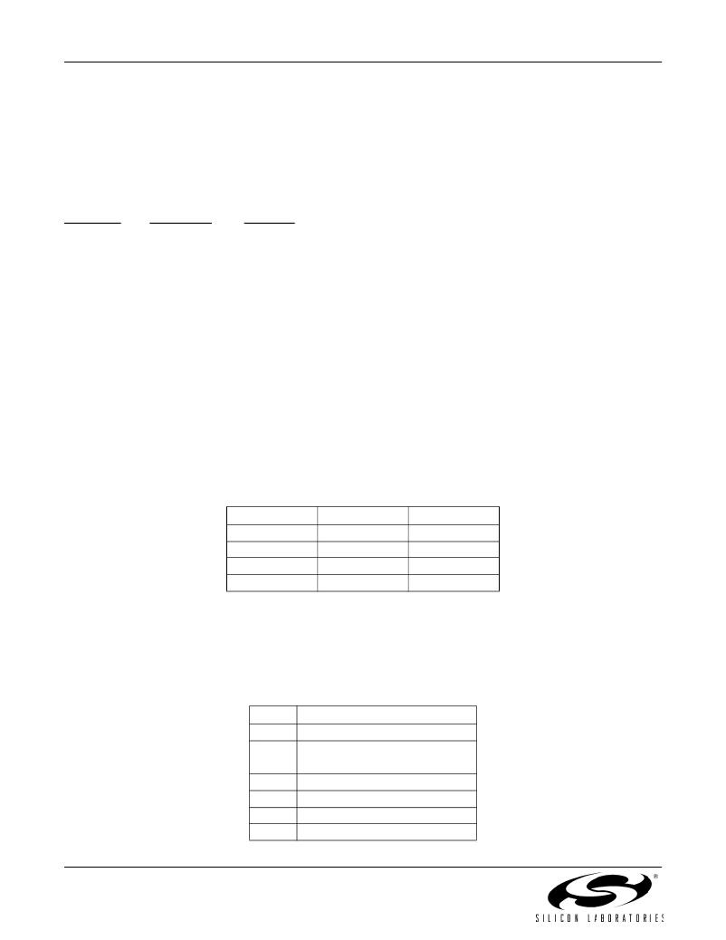
�Freq(MHz)�
�Digikey P/N�
�ECS P/N�
�22.1184�
�18.432�
�11.0592�
�X063-ND�
�X146-ND�
�X089-ND�
�ECS-221-20-1�
�ECS-184-20-1�
�ECS-110.5-20-1�
�(20� pF� loading� capacitance)�
�(20� pF� loading� capacitance)�
�(20� pF� loading� capacitance)�
�6.2.� Switches� and� LEDs�
�Two� switches� are� provided� on� the� target� board.� Switch� SW1� is� connected� to� the� RESET� pin� of� the� C8051F2xx�
�device� on� the� target� board.� Pressing� SW1� puts� the� device� into� its� hardware-reset� state.� The� device� will� leave� the�
�reset� state� after� SW1� is� released.� Switch� SW2� is� connected� to� the� device’s� general� purpose� I/O� (GPIO)� pin� through�
�headers.� Pressing� SW2� generates� a� logic� low� signal� on� the� port� pin.� Remove� the� shorting� block� from� the� header� to�
�disconnect� SW2� from� the� port� pins.� The� port� pin� signal� is� also� routed� to� a� pin� on� the� J2� I/O� connector.� See� Table� 1�
�for� the� port� pins� and� headers� corresponding� to� each� switch.�
�Two� LEDs� are� also� provided� on� the� target� board.� The� red� LED� labeled� PWR� is� used� to� indicate� a� power� connection�
�to� the� target� board.� The� green� LED� labeled� with� a� port� pin� name� is� connected� to� the� device’s� GPIO� pin� through�
�headers.� Remove� the� shorting� block� from� the� header� to� disconnect� the� LED� from� the� port� pin.� The� port� pin� signal� is�
�also� routed� to� a� pin� on� the� J2� I/O� connector.� See� Table� 1� for� the� port� pins� and� headers� corresponding� to� each� LED.�
�Table� 1.� Target� Board� I/O� Descriptions�
�Description�
�SW1�
�SW2�
�Green� LED�
�Red� LED�
�I/O�
�Reset�
�P2.5�
�P2.4�
�PWR�
�Header�
�none�
�P2.5�
�LED�
�none�
�6.3.� Target� Board� JTAG� Interface� (J4)�
�The� JTAG� connector� (J4)� provides� access� to� the� JTAG� pins� of� the� C8051F2xx.� It� is� used� to� connect� the� Serial�
�Adapter� or� the� USB� Debug� Adapter� to� the� target� board� for� in-circuit� debugging� and� Flash� programming.� Table� 2�
�shows� the� JTAG� pin� definitions.�
�Table� 2.� JTAG� Connector� Pin� Descriptions�
�6�
�Pin� #�
�1�
�2,� 3,� 9�
�4�
�5�
�6�
�7�
�8,� 10�
�Description�
�+3VD� (+3.3VDC)�
�GND� (Ground)�
�TCK�
�TMS�
�TDO�
�TDI�
�Not� Connected�
�Rev.� 0.6�
�相关PDF资料 |
PDF描述 |
|---|---|
| EEM12DTMT-S273 | CONN EDGECARD 24POS R/A .156 SLD |
| EEC36DRYS | CONN EDGECARD 72POS DIP .100 SLD |
| GBM08DTMT-S273 | CONN EDGECARD 16POS R/A .156 SLD |
| MAX6430EHUS+T | IC MONITOR BAT LP SOT143-4 |
| ECM36DCCI | CONN EDGECARD 72POS R/A .156 SLD |
相关代理商/技术参数 |
参数描述 |
|---|---|
| C8051F206DK-T | 功能描述:DEV KIT FOR C8051F206 RoHS:否 类别:编程器,开发系统 >> 过时/停产零件编号 系列:- 标准包装:1 系列:- 类型:MCU 适用于相关产品:Freescale MC68HC908LJ/LK(80-QFP ZIF 插口) 所含物品:面板、缆线、软件、数据表和用户手册 其它名称:520-1035 |
| C8051F206DK-U | 功能描述:DEV KIT FOR C8051F206 RoHS:否 类别:编程器,开发系统 >> 过时/停产零件编号 系列:- 标准包装:1 系列:- 类型:MCU 适用于相关产品:Freescale MC68HC908LJ/LK(80-QFP ZIF 插口) 所含物品:面板、缆线、软件、数据表和用户手册 其它名称:520-1035 |
| C8051F206-GQ | 功能描述:8位微控制器 -MCU 8KB 12ADC 1KRam 48P MCU RoHS:否 制造商:Silicon Labs 核心:8051 处理器系列:C8051F39x 数据总线宽度:8 bit 最大时钟频率:50 MHz 程序存储器大小:16 KB 数据 RAM 大小:1 KB 片上 ADC:Yes 工作电源电压:1.8 V to 3.6 V 工作温度范围:- 40 C to + 105 C 封装 / 箱体:QFN-20 安装风格:SMD/SMT |
| C8051F206-GQR | 功能描述:8位微控制器 -MCU 8KB 12ADC 1KRam 48P Tape and Reel RoHS:否 制造商:Silicon Labs 核心:8051 处理器系列:C8051F39x 数据总线宽度:8 bit 最大时钟频率:50 MHz 程序存储器大小:16 KB 数据 RAM 大小:1 KB 片上 ADC:Yes 工作电源电压:1.8 V to 3.6 V 工作温度范围:- 40 C to + 105 C 封装 / 箱体:QFN-20 安装风格:SMD/SMT |
| C8051F206R | 功能描述:8位微控制器 -MCU T-121280 Ram 48Pin RoHS:否 制造商:Silicon Labs 核心:8051 处理器系列:C8051F39x 数据总线宽度:8 bit 最大时钟频率:50 MHz 程序存储器大小:16 KB 数据 RAM 大小:1 KB 片上 ADC:Yes 工作电源电压:1.8 V to 3.6 V 工作温度范围:- 40 C to + 105 C 封装 / 箱体:QFN-20 安装风格:SMD/SMT |
发布紧急采购,3分钟左右您将得到回复。