- 您现在的位置:买卖IC网 > PDF目录379948 > COP8SGA040N9 (National Semiconductor Corporation) 8-Bit CMOS ROM Based and OTP Microcontrollers with 8k to 32k Memory, Two Comparators and USART PDF资料下载
参数资料
| 型号: | COP8SGA040N9 |
| 厂商: | National Semiconductor Corporation |
| 英文描述: | 8-Bit CMOS ROM Based and OTP Microcontrollers with 8k to 32k Memory, Two Comparators and USART |
| 中文描述: | 8位的CMOS基于ROM和OTP微控制器具有8K到32K的内存,2个比较器和USART |
| 文件页数: | 18/62页 |
| 文件大小: | 913K |
| 代理商: | COP8SGA040N9 |
第1页第2页第3页第4页第5页第6页第7页第8页第9页第10页第11页第12页第13页第14页第15页第16页第17页当前第18页第19页第20页第21页第22页第23页第24页第25页第26页第27页第28页第29页第30页第31页第32页第33页第34页第35页第36页第37页第38页第39页第40页第41页第42页第43页第44页第45页第46页第47页第48页第49页第50页第51页第52页第53页第54页第55页第56页第57页第58页第59页第60页第61页第62页
5.0 Functional Description
(Continued)
programmed to 0 for all other applications.
Enable full port F capability.
HALT mode disabled.
HALT mode enabled.
= 0
= 1
= 0
Bit 0
5.6 USER STORAGE SPACE IN EPROM
The ECON register is outside of the normal address range of
the ROM and can not be accessed by the executing soft-
ware.
The COP8 assembler defines a special ROM section type,
CONF, into which the ECON may be coded. Both ECON and
User Data are programmed automatically by programmers
that are certified by National.
The following examples illustrate the declaration of ECON
and the User information.
Syntax:
[label:] .sect
econ, conf
.db
value
;1 byte,
;configures options
<user information>
.endsect
; up to 8 bytes
Example: The following sets a value in the ECON register
and User Identification for a COP8SGR728M7. The ECON
bit values shown select options: Power-on enabled, Security
disabled, Crystal oscillator with on-chip bias disabled,
WATCHDOG enabled and HALT mode enabled.
.sect
econ, conf
.db
0x55
;por, xtal, wd, halt
.db
'my v1.00' ;user data declaration
.endsect
.db
5.7 OTP SECURITY
The device has a security feature that, when enabled, pre-
vents external reading of the OTP program memory. The
security bit in the ECON register determines, whether secu-
rity is enabled or disabled. If the security feature is disabled,
the contents of the internal EPROM may be read.
If the security feature is enabled, then any attempt to
externally read the contents of the EPROM will result in
the value FF Hex being read from all program locations
Under no circumstances can a secured part be read.
In
addition, with the security feature enabled, the write opera-
tion to the EPROM program memory and ECON register is
inhibited. The ECON register is readable regardless of the
state of the security bit. The security bit, when set,
cannot
be erased,
even in windowed packages.
If the security bit
is set in a device in a windowed package, that device may be
erased but will not be further programmable.
If security is being used, it is recommended that all other bits
in the ECON register be programmed first. Then the security
bit can be programmed.
5.8 ERASURE CHARACTERISTICS
The erasure characteristics of the device are such that era-
sure begins to occur when exposed to light with wavelengths
shorter than approximately 4000 Angstroms (). It should be
noted that sunlight and certain types of fluorescent lamps
have wavelengths in the 3000 - 4000 range.
After programming, opaque labels should be placed over the
window of windowed devices to prevent unintentional era-
sure. Covering the window will also prevent temporary func-
tional failure due to the generation of photo currents.
The recommended erasure procedure for windowed devices
is exposure to short wave ultraviolet light which has a wave-
length of 2537 Angstroms (). The integrated dose (i.e. UV
intensity X exposure time) for erasure should be a minimum
of 15W-sec/cm
2
.
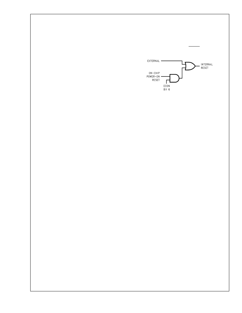
5.9 RESET
The devices are initialized when the RESET pin is pulled low
or the On-chip Power-On Reset is enabled.
The following occurs upon initialization:
Port L: TRI-STATE (High Impedance Input)
Port C: TRI-STATE (High Impedance Input)
Port G: TRI-STATE (High Impedance Input)
Port F: TRI-STATE (High Impedance Input)
Port D: HIGH
PC: CLEARED to 0000
PSW, CNTRL and ICNTRL registers: CLEARED
SIOR:
UNAFFECTED after RESET with power already applied
RANDOM after RESET at power-on
T2CNTRL: CLEARED
T3CNTRL: CLEARED
Accumulator, Timer 1, Timer 2 and Timer 3:
RANDOM after RESET with crystal clock option
(power already applied)
UNAFFECTED after RESET with R/C clock option
(power already applied)
RANDOM after RESET at power-on
WKEN, WKEDG: CLEARED
WKPND: RANDOM
SP (Stack Pointer):
Initialized to RAM address 06F Hex
B and X Pointers:
UNAFFECTED after RESET with power already applied
RANDOM after RESET at power-on
S Register: CLEARED
RAM:
UNAFFECTED after RESET with power already applied
RANDOM after RESET at power-on
USART:
PSR, ENU, ENUR, ENUI: Cleared except the TBMT bit
which is set to one.
COMPARATORS:
CMPSL; CLEARED
WATCHDOG (if enabled):
10131713
FIGURE 8. Reset Logic
C
www.national.com
18
相关PDF资料 |
PDF描述 |
|---|---|
| COP8SGA040Q3 | LMH0046 HD/SD SDI Reclocker with Dual Differential Outputs; Package: TSSOP EXP PAD; No of Pins: 20 |
| COP8SGA040Q6 | 8-Bit CMOS ROM Based and OTP Microcontrollers with 8k to 32k Memory, Two Comparators and USART |
| COP8SGA040Q7 | 8-Bit CMOS ROM Based and OTP Microcontrollers with 8k to 32k Memory, Two Comparators and USART |
| COP8SGA040Q8 | 8-Bit CMOS ROM Based and OTP Microcontrollers with 8k to 32k Memory, Two Comparators and USART |
| COP8SGA040Q9 | 8-Bit CMOS ROM Based and OTP Microcontrollers with 8k to 32k Memory, Two Comparators and USART |
相关代理商/技术参数 |
参数描述 |
|---|---|
| COP8SGA040Q3 | 制造商:NSC 制造商全称:National Semiconductor 功能描述:8-Bit CMOS ROM Based and OTP Microcontrollers with 8k to 32k Memory, Two Comparators and USART |
| COP8SGA040Q6 | 制造商:NSC 制造商全称:National Semiconductor 功能描述:8-Bit CMOS ROM Based and OTP Microcontrollers with 8k to 32k Memory, Two Comparators and USART |
| COP8SGA040Q7 | 制造商:NSC 制造商全称:National Semiconductor 功能描述:8-Bit CMOS ROM Based and OTP Microcontrollers with 8k to 32k Memory, Two Comparators and USART |
| COP8SGA040Q8 | 制造商:NSC 制造商全称:National Semiconductor 功能描述:8-Bit CMOS ROM Based and OTP Microcontrollers with 8k to 32k Memory, Two Comparators and USART |
| COP8SGA040Q9 | 制造商:NSC 制造商全称:National Semiconductor 功能描述:8-Bit CMOS ROM Based and OTP Microcontrollers with 8k to 32k Memory, Two Comparators and USART |
发布紧急采购,3分钟左右您将得到回复。