- 您现在的位置:买卖IC网 > PDF目录21105 > LTC2630CSC6-HZ10#TRMPBF (Linear Technology)IC DAC 10BIT R-R SC70-6 PDF资料下载
参数资料
| 型号: | LTC2630CSC6-HZ10#TRMPBF |
| 厂商: | Linear Technology |
| 文件页数: | 5/22页 |
| 文件大小: | 0K |
| 描述: | IC DAC 10BIT R-R SC70-6 |
| 产品培训模块: | LTC263x 12-, 10-, and 8-Bit VOUT DAC Family |
| 标准包装: | 1 |
| 设置时间: | 3.9µs |
| 位数: | 10 |
| 数据接口: | 串行 |
| 转换器数目: | 1 |
| 电压电源: | 单电源 |
| 功率耗散(最大): | 480µW |
| 工作温度: | 0°C ~ 70°C |
| 安装类型: | 表面贴装 |
| 封装/外壳: | 6-TSSOP,SC-88,SOT-363 |
| 供应商设备封装: | SC-70-6 |
| 包装: | 标准包装 |
| 输出数目和类型: | 1 电压,单极 |
| 采样率(每秒): | * |
| 产品目录页面: | 1351 (CN2011-ZH PDF) |
| 其它名称: | LTC2630CSC6-HZ10#TRMPBFDKR |
LTC2630
13
2630ff
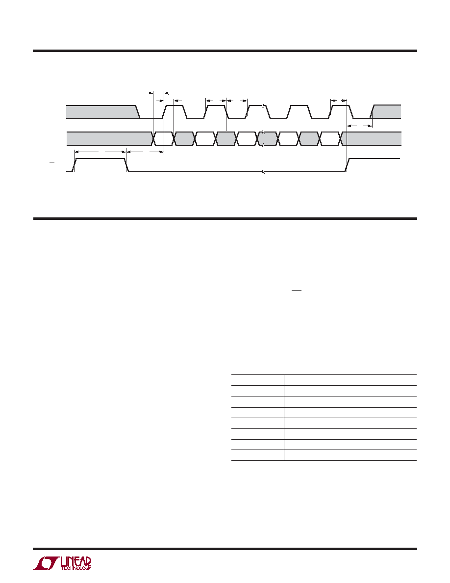
timing Diagram
The LTC2630 is a family of single voltage output DACs in
6-lead SC70 packages. Each DAC can operate rail-to-rail
referenced to the input supply, or with its full-scale voltage
set by an integrated reference. Twelve combinations of
accuracy (12-, 10-, and 8-bit), power-on reset value (zero
or mid-scale), and full-scale voltage (2.5V or 4.096V) are
available. The LTC2630 is controlled using a 3-wire SPI/
MICROWIRE compatible interface.
Power-On Reset
The LTC2630-HZ/-LZ clear the output to zero scale when
power is first applied, making system initialization con-
sistent and repeatable.
For some applications, downstream circuits are active
during DAC power-up, and may be sensitive to nonzero
outputs from the DAC during this time. The LTC2630
contains circuitry to reduce the power-on glitch: the
analog output typically rises less than 5mV above zero
scale during power on if the power supply is ramped
to 5V in 1ms or more. In general, the glitch amplitude
decreases as the power supply ramp time is increased.
See “Power-On Reset Glitch” in the Typical Performance
Characteristics section.
The LTC2630-HM/-LM provide an alternative reset, set-
ting the output to mid-scale when power is first applied.
SDI
CS/LD
SCK
t2
t10
t5
t7
t6
t1
t3
t4
1
2
3
23
24
2630 F01
operation
Transfer Function
The digital-to-analog transfer function is
VOUT(IDEAL) =
k
2N
VREF
where k is the decimal equivalent of the binary DAC
input code, N is the resolution, and VREF is either 2.5V
(LTC2630-L) or 4.096V (LTC2630-H) in internal refer-
ence mode, and VCC in Supply as reference mode.
Table 1. Command Codes
Command*
C3 C2 C1 C0
0
Write to Input Register
0
1
Update (Power up) DAC Register
0
1
Write to and Update (Power up) DAC Register
0
1
0
Power down
0
1
0
Select Internal Reference (Power-on Reset Default)
0
1
Select Supply as Reference (VREF = VCC)
*Command codes not shown are reserved and should not be used.
Figure 1. Serial Interface Timing
相关PDF资料 |
PDF描述 |
|---|---|
| P51-50-A-Z-I36-4.5OVP-000-000 | SENSOR 50PSI 1/4-18NPT .5-4.5V |
| REC5-4809SRWZ/H6/A/SMD-R | CONV DC/DC 5W 18-72VIN 09VOUT |
| P51-100-S-S-M12-20MA-000-000 | SENSOR 100PSIS 1/4 NPT 4-20 MA |
| P51-50-A-B-P-4.5OVP-000-000 | SENSOR 50PSI 1/8-27NPT .5-4.5V |
| P51-15-A-Y-I36-4.5OVP-000-000 | SENSOR 15PSI 7/16-20-2B .5-4.5V |
相关代理商/技术参数 |
参数描述 |
|---|---|
| CS5531 | 制造商:CIRRUS 制造商全称:Cirrus Logic 功能描述:16 BIT AND 24 BIT ADCS WITH ULTRA LOW NOISE PGIA |
| CS5531_08 | 制造商:CIRRUS 制造商全称:Cirrus Logic 功能描述:16-bit and 24-bit ADCs with Ultra-low-noise PGIA |
| CS5531-AS | 功能描述:模数转换器 - ADC 2-Ch 16-Bit ADCs w/ Ultra Low Noise PGIA RoHS:否 制造商:Texas Instruments 通道数量:2 结构:Sigma-Delta 转换速率:125 SPs to 8 KSPs 分辨率:24 bit 输入类型:Differential 信噪比:107 dB 接口类型:SPI 工作电源电压:1.7 V to 3.6 V, 2.7 V to 5.25 V 最大工作温度:+ 85 C 安装风格:SMD/SMT 封装 / 箱体:VQFN-32 |
| CS5531-ASR | 功能描述:模数转换器 - ADC IC 16-Bit ADCs w/UltraLw Noise PGIA RoHS:否 制造商:Texas Instruments 通道数量:2 结构:Sigma-Delta 转换速率:125 SPs to 8 KSPs 分辨率:24 bit 输入类型:Differential 信噪比:107 dB 接口类型:SPI 工作电源电压:1.7 V to 3.6 V, 2.7 V to 5.25 V 最大工作温度:+ 85 C 安装风格:SMD/SMT 封装 / 箱体:VQFN-32 |
| CS5531-ASZ | 功能描述:模数转换器 - ADC 2-Ch 16-Bit ADCs w/ Ultra Low Noise PGIA RoHS:否 制造商:Texas Instruments 通道数量:2 结构:Sigma-Delta 转换速率:125 SPs to 8 KSPs 分辨率:24 bit 输入类型:Differential 信噪比:107 dB 接口类型:SPI 工作电源电压:1.7 V to 3.6 V, 2.7 V to 5.25 V 最大工作温度:+ 85 C 安装风格:SMD/SMT 封装 / 箱体:VQFN-32 |
发布紧急采购,3分钟左右您将得到回复。