- 您现在的位置:买卖IC网 > PDF目录379057 > CY7C1148V18-333BZC (CYPRESS SEMICONDUCTOR CORP) 18-Mbit DDR-II+ SRAM 2-Word Burst Architecture (2.0 Cycle Read Latency) PDF资料下载
参数资料
| 型号: | CY7C1148V18-333BZC |
| 厂商: | CYPRESS SEMICONDUCTOR CORP |
| 元件分类: | DRAM |
| 英文描述: | 18-Mbit DDR-II+ SRAM 2-Word Burst Architecture (2.0 Cycle Read Latency) |
| 中文描述: | 1M X 18 DDR SRAM, 0.45 ns, PBGA165 |
| 封装: | 13 X 15 MM, 1.40 MM HEIGHT, MO-216, FBGA-165 |
| 文件页数: | 6/27页 |
| 文件大小: | 969K |
| 代理商: | CY7C1148V18-333BZC |
第1页第2页第3页第4页第5页当前第6页第7页第8页第9页第10页第11页第12页第13页第14页第15页第16页第17页第18页第19页第20页第21页第22页第23页第24页第25页第26页第27页
CY7C1146V18
CY7C1157V18
CY7C1148V18
CY7C1150V18
Document Number: 001-06621 Rev. *C
Page 6 of 27
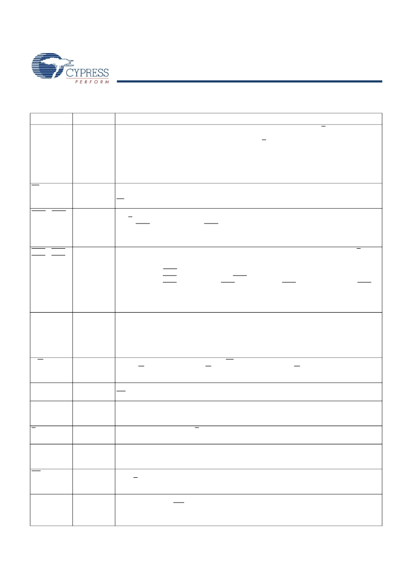
Pin Definitions
Pin Name
IO
Pin Description
DQ
[x:0]
Input Output-
Synchronous
Data Input Output Signals
. Inputs are sampled on the rising edge of K and K clocks when write
operations are valid. These pins drive out the requested data when a read operation is active. Valid
data is driven out on the rising edge of both the K and K clocks when read operations are active.
When read access is deselected, Q
[x:0]
are automatically tri-stated.
CY7C1146V18
DQ
[7:0]
CY7C1157V18
DQ
[8:0]
CY7C1148V18
DQ
[17:0]
CY7C1150V18
DQ
[35:0]
Synchronous Load
. This input is brought LOW when a bus cycle sequence is to be defined. This
definition includes address and read/write direction. All transactions operate on a burst of two data.
LD must meet the setup and hold times around edge of K.
LD
Input-
Synchronous
NWS
0
, NWS
1
,
Input-
Synchronous
Nibble Write Select 0, 1
Active LOW
.(
CY7C1146V18
Only
) Sampled on the rising edge of the K
and K clocks when the write operation is active. It is used to select the nibble that is written into the
device NWS
0
controls D
[3:0]
and NWS
1
controls D
[7:4]
.
All the Nibble Write Selects are sampled on the same edge as the data. Deselecting a Nibble Write
Select causes the corresponding nibble of data to be ignored and not written into the device.
BWS
0
, BWS
1
,
BWS
2
, BWS
3
Input-
Synchronous
Byte Write Select 0, 1, 2, and 3
Active LOW
. Sampled on the rising edge of the K and K clocks
when the Write operation is active. It is used to select the byte that is written into the device when
the current portion of the write operation is active. Bytes not written remain unaltered.
CY7C1157V18
BWS
0
controls D
[8:0]
CY7C1148V18
BWS
0
controls D
[8:0]
, and BWS
1
controls D
[17:9].
CY7C1148V18
BWS
0
controls D
[8:0]
, BWS
1
controls D
[17:9]
, BWS
2
controls D
[26:18]
, and BWS
3
controls D
[35:27]
.
All the Byte Write Selects are sampled on the same edge as the data. Deselecting a Byte Write Select
causes the corresponding byte of data to be ignored and not written into the device.
A
Input-
Synchronous
Address Inputs
. Sampled on the rising edge of the K clock during active read and write operations.
These address inputs are multiplexed for both read and write operations. Internally, the device is
organized as 2M x 8 (two arrays each of1M x 8) for CY7C1146V18, 2M x 9 (two arrays each of 1M
x 9) for CY7C1157V18, 1M x 18 (two arrays each of 512K x 18) for CY7C1148V18, and 512K x 36
(two arrays each of 256K x 18) for CY7C1150V18. All the address inputs are ignored when the
appropriate port is deselected.
R/W
Input-
Synchronous
Synchronous Read/Write Input
. When LD is LOW, this input designates the access type (read
when R/W is HIGH, write when R/W is LOW) for loaded address. R/W must meet the setup and hold
times around edge of K.
QVLD
Valid Output
Indicator
Valid Output Indicator
. The Q Valid indicates valid output data. QVLD is edge aligned with CQ and
CQ.
K
Input-
Clock
Positive Input Clock Input
. The rising edge of K is used to capture synchronous inputs to the device
and to drive out data through Q
[x:0]
when in single clock mode. All accesses are initiated on the rising
edge of K.
K
Input-
Clock
Negative Input Clock Input
. K is used to capture synchronous inputs being presented to the device
and to drive out data through Q
[x:0]
when in single clock mode.
CQ
Clock Output
Synchronous Echo Clock Outputs
. This is a free running clock and is synchronized to the input
clock (K) of the DDR-II+. The timings for the echo clocks are shown in the
“Switching Characteristics”
on page 22
.
CQ
Clock Output
Synchronous Echo Clock Outputs
. This is a free running clock and is synchronized to the input
clock (K) of the DDR-II+. The timings for the echo clocks are shown in the
“Switching Characteristics”
on page 22
.
ZQ
Input
Output Impedance Matching Input
. This input is used to tune the device outputs to the system data
bus impedance. CQ, CQ, and Q
[x:0]
output impedance are set to 0.2 x RQ, where RQ is a resistor
connected between ZQ and ground. Alternatively, connect this pin directly to V
DDQ
, which enables
the minimum impedance mode. This pin cannot be connected directly to GND or left unconnected.
[+] Feedback
相关PDF资料 |
PDF描述 |
|---|---|
| CY7C1148V18-333BZI | 18-Mbit DDR-II+ SRAM 2-Word Burst Architecture (2.0 Cycle Read Latency) |
| CY7C1148V18-333BZXC | 18-Mbit DDR-II+ SRAM 2-Word Burst Architecture (2.0 Cycle Read Latency) |
| CY7C1148V18-333BZXI | 18-Mbit DDR-II+ SRAM 2-Word Burst Architecture (2.0 Cycle Read Latency) |
| CY7C1148V18-375BZC | 18-Mbit DDR-II+ SRAM 2-Word Burst Architecture (2.0 Cycle Read Latency) |
| CY7C1148V18-375BZI | 18-Mbit DDR-II+ SRAM 2-Word Burst Architecture (2.0 Cycle Read Latency) |
相关代理商/技术参数 |
参数描述 |
|---|---|
| CY7C11501KV18-400BZXC | 功能描述:IC SRAM 18MBIT 400MHZ 165-FBGA RoHS:是 类别:集成电路 (IC) >> 存储器 系列:- 标准包装:150 系列:- 格式 - 存储器:EEPROMs - 串行 存储器类型:EEPROM 存储容量:4K (2 x 256 x 8) 速度:400kHz 接口:I²C,2 线串口 电源电压:2.5 V ~ 5.5 V 工作温度:-40°C ~ 85°C 封装/外壳:8-VFDFN 裸露焊盘 供应商设备封装:8-DFN(2x3) 包装:管件 产品目录页面:1445 (CN2011-ZH PDF) |
| CY7C11501KV18-400BZXI | 功能描述:IC SRAM 18MBIT 400MHZ 165-FBGA RoHS:是 类别:集成电路 (IC) >> 存储器 系列:- 标准包装:150 系列:- 格式 - 存储器:EEPROMs - 串行 存储器类型:EEPROM 存储容量:4K (2 x 256 x 8) 速度:400kHz 接口:I²C,2 线串口 电源电压:2.5 V ~ 5.5 V 工作温度:-40°C ~ 85°C 封装/外壳:8-VFDFN 裸露焊盘 供应商设备封装:8-DFN(2x3) 包装:管件 产品目录页面:1445 (CN2011-ZH PDF) |
| CY7C1150KV18-400BZC | 功能描述:静态随机存取存储器 18MB (512Kx36) 1.8v 400MHz DDR II 静态随机存取存储器 RoHS:否 制造商:Cypress Semiconductor 存储容量:16 Mbit 组织:1 M x 16 访问时间:55 ns 电源电压-最大:3.6 V 电源电压-最小:2.2 V 最大工作电流:22 uA 最大工作温度:+ 85 C 最小工作温度:- 40 C 安装风格:SMD/SMT 封装 / 箱体:TSOP-48 封装:Tray |
| CY7C1150KV18-400BZXC | 功能描述:静态随机存取存储器 18MB (512Kx36) 1.8v 400MHz DDR II 静态随机存取存储器 RoHS:否 制造商:Cypress Semiconductor 存储容量:16 Mbit 组织:1 M x 16 访问时间:55 ns 电源电压-最大:3.6 V 电源电压-最小:2.2 V 最大工作电流:22 uA 最大工作温度:+ 85 C 最小工作温度:- 40 C 安装风格:SMD/SMT 封装 / 箱体:TSOP-48 封装:Tray |
| CY7C1150KV18-400BZXI | 功能描述:静态随机存取存储器 18MB (512Kx36) 1.8v 400MHz DDR II 静态随机存取存储器 RoHS:否 制造商:Cypress Semiconductor 存储容量:16 Mbit 组织:1 M x 16 访问时间:55 ns 电源电压-最大:3.6 V 电源电压-最小:2.2 V 最大工作电流:22 uA 最大工作温度:+ 85 C 最小工作温度:- 40 C 安装风格:SMD/SMT 封装 / 箱体:TSOP-48 封装:Tray |
发布紧急采购,3分钟左右您将得到回复。