- 您现在的位置:买卖IC网 > PDF目录378509 > CY7C1487V25-133BGI (CYPRESS SEMICONDUCTOR CORP) 72-Mbit (2M x 36/4M x 18/1M x 72) Flow-Through SRAM PDF资料下载
参数资料
| 型号: | CY7C1487V25-133BGI |
| 厂商: | CYPRESS SEMICONDUCTOR CORP |
| 元件分类: | DRAM |
| 英文描述: | 72-Mbit (2M x 36/4M x 18/1M x 72) Flow-Through SRAM |
| 中文描述: | 1M X 72 CACHE SRAM, 6.5 ns, PBGA209 |
| 封装: | 14 X 22 MM, 1.76 MM HEIGHT, FBGA-209 |
| 文件页数: | 7/30页 |
| 文件大小: | 1028K |
| 代理商: | CY7C1487V25-133BGI |
第1页第2页第3页第4页第5页第6页当前第7页第8页第9页第10页第11页第12页第13页第14页第15页第16页第17页第18页第19页第20页第21页第22页第23页第24页第25页第26页第27页第28页第29页第30页
CY7C1481V25
CY7C1483V25
CY7C1487V25
Document #: 38-05281 Rev. *H
Page 7 of 30
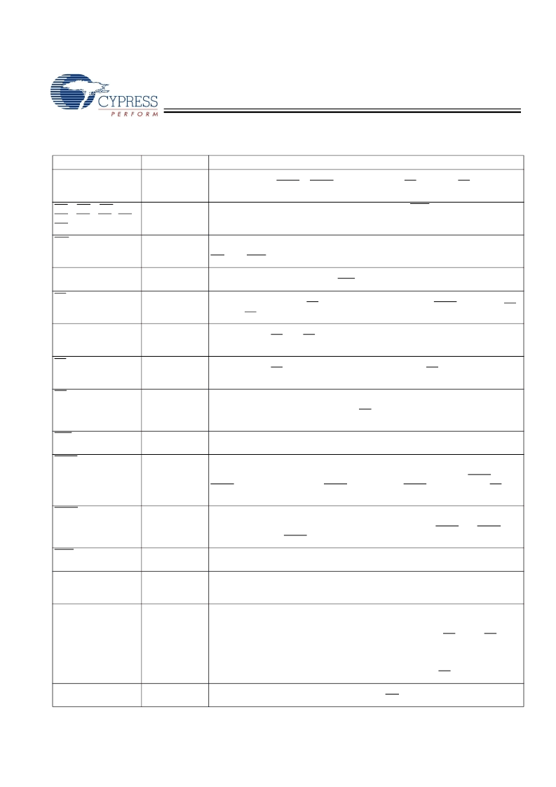
Pin Definitions
Pin Name
I/O
Description
A
0
, A
1
, A
Input-
Synchronous
Address Inputs used to select one of the address locations
. Sampled at the rising
edge of the CLK if ADSP or ADSC is active LOW, and CE
1
,
CE
2
, and
CE
3
are sampled
active. A
[1:0]
feed the 2-bit counter.
Byte Write Select Inputs, active LOW
. Qualified with BWE to conduct byte writes to
the SRAM. Sampled on the rising edge of CLK.
BW
A
, BW
B
, BW
C
,
BW
D
, BW
E
, BW
F
, BW
G
,
BW
H
GW
Input-
Synchronous
Input-
Synchronous
Global Write Enable Input, active LOW
. When asserted LOW on the rising edge of
CLK, a global write is conducted (ALL bytes are written, regardless of the values on
BW
X
and BWE).
Clock Input
. Used to capture all synchronous inputs to the device. Also used to
increment the burst counter when ADV is asserted LOW, during a burst operation.
CLK
Input-
Clock
CE
1
Input-
Synchronous
Chip Enable 1 Input, active LOW
. Sampled on the rising edge of CLK. Used in
conjunction with CE
2
and CE
3
to select/deselect the device. ADSP is ignored if CE
1
is HIGH. CE
1
is sampled only when a new external address is loaded.
Chip Enable 2 Input, active HIGH
. Sampled on the rising edge of CLK. Used in
conjunction with CE
1
and CE
3
to select/deselect the device. CE
2
is sampled only when
a new external address is loaded.
CE
2
Input-
Synchronous
CE
3
Input-
Synchronous
Chip Enable 3 Input, active LOW
. Sampled on the rising edge of CLK. Used in
conjunction with CE
1
and CE
2
to select/deselect the device. CE
3
is sampled only when
a new external address is loaded.
OE
Input-
Asynchronous
Output Enable, asynchronous input, active LOW
. Controls the direction of the IO
pins. When LOW, the IO pins behave as outputs. When deasserted HIGH, IO pins
are tri-stated, and act as input data pins. OE is masked during the first clock of a read
cycle when emerging from a deselected state.
ADV
Input-
Synchronous
Advance Input signal, sampled on the rising edge of CLK
. When asserted, it
automatically increments the address in a burst cycle.
ADSP
Input-
Synchronous
Address Strobe from Processor, sampled on the rising edge of CLK, active
LOW
. When asserted LOW, addresses presented to the device are captured in the
address registers. A
[1:0]
are also loaded into the burst counter. When ADSP and
ADSC are both asserted, only ADSP is recognized. ASDP is ignored when CE
1
is
deasserted HIGH.
ADSC
Input-
Synchronous
Address Strobe from Controller, sampled on the rising edge of CLK, active LOW
.
When asserted LOW, addresses presented to the device are captured in the address
registers. A
are also loaded into the burst counter. When ADSP and ADSC are
both asserted, only ADSP is recognized.
BWE
Input-
Synchronous
Byte Write Enable Input, active LOW
. Sampled on the rising edge of CLK. This
signal must be asserted LOW to conduct a byte write.
ZZ
Input-
Asynchronous
ZZ “sleep” Input, active HIGH
. When asserted HIGH places the device in a
non-time-critical “sleep” condition with data integrity preserved. For normal operation,
this pin must be LOW or left floating. ZZ pin has an internal pull down.
DQ
s
I/O-
Synchronous
Bidirectional Data IO Lines
. As inputs, they feed into an on-chip data register that
is triggered by the rising edge of CLK. As outputs, they deliver the data contained in
the memory location specified by the addresses presented during the previous clock
rise of the read cycle. The direction of the pins is controlled by OE. When OE is
asserted LOW, the pins behave as outputs. When HIGH, DQ
s
and DQP
X
are placed
in a tri-state condition. The outputs are automatically tri-stated during the data portion
of a write sequence, during the first clock when emerging from a deselected state,
and when the device is deselected, regardless of the state of OE.
DQP
X
I/O-
Synchronous
Bidirectional Data Parity IO Lines.
Functionally, these signals are identical to DQ
s
.
During write sequences, DQP
x
is controlled by BW
X
,
correspondingly.
[+] Feedback
相关PDF资料 |
PDF描述 |
|---|---|
| CY7C1487V25-133BGXC | 72-Mbit (2M x 36/4M x 18/1M x 72) Flow-Through SRAM |
| CY7C1487V25-133BGXI | 72-Mbit (2M x 36/4M x 18/1M x 72) Flow-Through SRAM |
| CY7C1481V25-100AXC | 72-Mbit (2M x 36/4M x 18/1M x 72) Flow-Through SRAM |
| CY7C1481V25-100AXI | 72-Mbit (2M x 36/4M x 18/1M x 72) Flow-Through SRAM |
| CY7C1481V25-100BZC | 72-Mbit (2M x 36/4M x 18/1M x 72) Flow-Through SRAM |
相关代理商/技术参数 |
参数描述 |
|---|---|
| CY7C149 WAF | 制造商:Cypress Semiconductor 功能描述: |
| CY7C149-45PC | 功能描述:1KX4 18-PIN SRAM RoHS:是 类别:集成电路 (IC) >> 存储器 系列:- 标准包装:1,000 系列:- 格式 - 存储器:EEPROMs - 串行 存储器类型:EEPROM 存储容量:4K (512 x 8) 速度:400kHz 接口:I²C,2 线串口 电源电压:2.7 V ~ 5.5 V 工作温度:-40°C ~ 85°C 封装/外壳:8-SOIC(0.173",4.40mm 宽) 供应商设备封装:8-MFP 包装:带卷 (TR) |
| CY7C150-10DC | 制造商:Rochester Electronics LLC 功能描述:- Bulk |
| CY7C150-15PC | 制造商:Rochester Electronics LLC 功能描述:4K (1K X 4)- 24 PIN 300 MIL SEPARATE I/O & RESET SRAM - Bulk |
| CY7C15025PC | 制造商:CYPRESS 功能描述:* |
发布紧急采购,3分钟左右您将得到回复。