- 您现在的位置:买卖IC网 > PDF目录379092 > CY7C4225-15JI (CYPRESS SEMICONDUCTOR CORP) 64/256/512/1K/2K/4K x18 Low-Voltage Synchronous FIFOs PDF资料下载
参数资料
| 型号: | CY7C4225-15JI |
| 厂商: | CYPRESS SEMICONDUCTOR CORP |
| 元件分类: | DRAM |
| 英文描述: | 64/256/512/1K/2K/4K x18 Low-Voltage Synchronous FIFOs |
| 中文描述: | 1K X 18 OTHER FIFO, 10 ns, PQCC68 |
| 封装: | PLASTIC, LCC-68 |
| 文件页数: | 14/25页 |
| 文件大小: | 409K |
| 代理商: | CY7C4225-15JI |
CY7C4425/4205/4215
CY7C4225/4235/4245
14
Architecture
The CY7C42X5 consists of an array of 64 to 4K words of 18
bits each (implemented by a dual-port array of SRAM cells), a
read pointer, a write pointer, control signals (RCLK, WCLK,
REN, WEN, RS), and flags (EF, PAE, HF, PAF, FF). The
CY7C42X5 also includes the control signals WXI, RXI, WXO,
RXO for depth expansion.
Resetting the FIFO
Upon power-up, the FIFO must be reset with a Reset (RS)
cycle. This causes the FIFO to enter the Empty condition sig-
nified by EF being LOW. All data outputs go LOW after the
falling edge of RS only if OE is asserted. In order for the FIFO
to reset to its default state, a falling edge must occur on RS
and the user must not read or write while RS is LOW.
FIFO Operation
When the WEN signal is active (LOW), data present on the
D
0–17
pins is written into the FIFO on each rising edge of the
WCLK signal. Similarly, when the REN signal is active LOW,
data in the FIFO memory will be presented on the Q
0–17
out-
puts. New data will be presented on each rising edge of RCLK
while REN is active LOW and OE is LOW. REN must set up
tENS before RCLK for it to be a valid read function. WEN must
occur tENS before WCLK for it to be a valid write function.
An output enable (OE) pin is provided to three-state the Q
0–17
outputs when OE is deasserted. When OE is enabled (LOW),
data in the output register will be available to the Q
0–17
outputs
after t
OE
. If devices are cascaded, the OE function will only
output data on the FIFO that is read enabled.
The FIFO contains overflow circuitry to disallow additional
writes when the FIFO is full, and underflow circuitry to disallow
additional reads when the FIFO is empty. An empty FIFO
maintains the data of the last valid read on its Q
0–17
outputs
even after additional reads occur.
Programming
The CY7C42X5 devices contain two 12-bit offset registers.
Data present on D
0–11
during a program write will determine
the distance from Empty (Full) that the Almost Empty (Almost
Full) flags become active. If the user elects not to program the
FIFO’s flags, the default offset values are used (see Table 2).
When the Load LD pin is set LOW and WEN is set LOW, data
on the inputs D
0–11
is written into the Empty offset register on
the first LOW-to-HIGH transition of the write clock (WCLK).
When the LD pin and WEN are held LOW then data is written
into the Full offset register on the second LOW-to-HIGH tran-
sition of the write clock (WCLK). The third transition of the write
clock (WCLK) again writes to the Empty offset register (see
Table 1). Writing all offset registers does not have to occur at
one time. One or two offset registers can be written and then,
by bringing the LD pin HIGH, the FIFO is returned to normal
read/write operation. When the LD pin is set LOW, and WEN
is LOW, the next offset register in sequence is written.
The contents of the offset registers can be read on the output
lines when the LD pin is set LOW and REN is set LOW; then,
data can be read on the LOW-to-HIGH transition of the read
clock (RCLK).
Flag Operation
The CY7C42X5 devices provide five flag pins to indicate the
condition of the FIFO contents. Empty and Full are synchro-
nous. PAE and PAF are synchronous if V
CC
/SMODE is tied to
V
SS
.
Full Flag
The Full Flag (FF) will go LOW when device is Full. Write op-
erations are inhibited whenever FF is LOW regardless of the
state of WEN. FF is synchronized to WCLK, i.e., it is exclusive-
ly updated by each rising edge of WCLK.
Empty Flag
The Empty Flag (EF) will go LOW when the device is empty.
Read operations are inhibited whenever EF is LOW, regard-
less of the state of REN. EF is synchronized to RCLK, i.e., it is
exclusively updated by each rising edge of RCLK.
Programmable Almost Empty/Almost Full Flag
The CY7C42X5 features programmable Almost Empty and Al-
most Full Flags. Each flag can be programmed (described in
the Programming section) a specific distance from the corre-
sponding boundary flags (Empty or Full). When the FIFO con-
tains the number of words or fewer for which the flags have
been programmed, the PAF or PAE will be asserted, signifying
that the FIFO is either Almost Full or Almost Empty. See Table
2 for a description of programmable flags.
When the SMODE pin is tied LOW, the PAF flag signal transi-
tion is caused by the rising edge of the write clock and the PAE
flag transition is caused by the rising edge of the read clock.
Retransmit
The retransmit feature is beneficial when transferring packets
of data. It enables the receipt of data to be acknowledged by
the receiver and retransmitted if necessary.
The Retransmit (RT) input is active in the standalone and width
expansion modes. The retransmit feature is intended for use
when a number of writes equal to or less than the depth of the
FIFO have occurred since the last RS cycle. A HIGH pulse on
RT resets the internal read pointer to the first physical location
of the FIFO. WCLK and RCLK may be free running but must
be disabled during and t
RTR
after the retransmit pulse. With
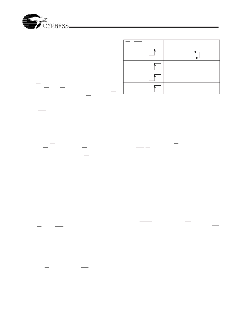
Table 1. Write Offset Register
LD
0
WEN
0
WCLK
[36]
Selection
Writing to offset registers:
Empty Offset
Full Offset
0
1
No Operation
1
0
Write Into FIFO
1
1
No Operation
Note:
36. The same selection sequence applies to reading from the registers. REN
is enabled and read is performed on the LOW-to-HIGH transition of RCLK.
相关PDF资料 |
PDF描述 |
|---|---|
| CY7C4225-25AC | 64/256/512/1K/2K/4K x18 Low-Voltage Synchronous FIFOs |
| CY7C4225-25AI | 64/256/512/1K/2K/4K x18 Low-Voltage Synchronous FIFOs |
| CY7C4225-25ASC | 64/256/512/1K/2K/4K x18 Low-Voltage Synchronous FIFOs |
| CY7C4225-25ASI | 64/256/512/1K/2K/4K x18 Low-Voltage Synchronous FIFOs |
| CY7C4225-25JC | 64/256/512/1K/2K/4K x18 Low-Voltage Synchronous FIFOs |
相关代理商/技术参数 |
参数描述 |
|---|---|
| CY7C422525AC | 制造商:Cypress Semiconductor 功能描述: |
| CY7C4225-25AC | 制造商:Rochester Electronics LLC 功能描述:- Bulk |
| CY7C4225-25JC | 制造商:Rochester Electronics LLC 功能描述:- Bulk |
| CY7C4225V-15ASC | 功能描述:IC SYNC FIFO MEM 1KX18 64LQFP RoHS:否 类别:集成电路 (IC) >> 逻辑 - FIFO 系列:CY7C 标准包装:15 系列:74F 功能:异步 存储容量:256(64 x 4) 数据速率:- 访问时间:- 电源电压:4.5 V ~ 5.5 V 工作温度:0°C ~ 70°C 安装类型:通孔 封装/外壳:24-DIP(0.300",7.62mm) 供应商设备封装:24-PDIP 包装:管件 其它名称:74F433 |
| CY7C4225V-15ASXC | 功能描述:先进先出 1K X18 LO VLTG SYNC 先进先出 COM RoHS:否 制造商:IDT 电路数量: 数据总线宽度:18 bit 总线定向:Unidirectional 存储容量:4 Mbit 定时类型:Synchronous 组织:256 K x 18 最大时钟频率:100 MHz 访问时间:10 ns 电源电压-最大:3.6 V 电源电压-最小:6 V 最大工作电流:35 mA 最大工作温度:+ 85 C 封装 / 箱体:TQFP-80 封装: |
发布紧急采购,3分钟左右您将得到回复。