- 您现在的位置:买卖IC网 > PDF目录97912 > ENH057Q1-600 Low Noise LDO with Low IQ, High PSRR; Temperature Range: -40°C to 85°C; Package: 6-uTDFN T&R PDF资料下载
参数资料
| 型号: | ENH057Q1-600 |
| 英文描述: | Low Noise LDO with Low IQ, High PSRR; Temperature Range: -40°C to 85°C; Package: 6-uTDFN T&R |
| 中文描述: | 5.7inch的QVGA |
| 文件页数: | 17/21页 |
| 文件大小: | 322K |
| 代理商: | ENH057Q1-600 |
Original specifications created by Sharp.
5
Panelview (503) 690-2460 www.whiteedc.com
Panelview is a subsidiary of White Electronic Designs Corporation
ENH050Q1-320/450/600
Panelview
Enhancing the Vision
TFT-LCD PANEL DRIVING SECTION
Parameter
SymbolMIN
TYP
MAX
Unit
Remarks
DC bias voltage for common electrode driving signal
VCDC
0
+2.0
+3.0
V
DC component (15)
Terminal voltage applicable to brightness
VBRT
+2.0
+2.3
+2. 4
V
BACKLIGHT DRIVING SECTION
Parameter
SymbolMIN
TYP
MAX
Unit
Remarks
Lamp Voltage
VL7
550
610
670
Vrms
IL=6.5mArms
Lamp current
IL
3.0
6.5
7.0
mArms
normal operation
Lamp frequency
f L
20
70
KHz
Kickoff voltage
VS
1450
Vrms
Ta = +25°C
1500
Vrms
Ta = -30°C
Notes:
1. Power supply voltage should not be changed after adjusting VCDC.
2. VR1, VG1, VB1, VR2, VG2, VB2 terminals (Video signal)
3. VBS, VR1, VG1, VB1, VR2, VG2, VB2 terminals
4. HSY, VSY, NTP, VSW, HRV, VRV, SAM CLKC, CLK terminals
5. HSY, VSY, CLK terminals (output mode)
6. CLK terminals (output mode)
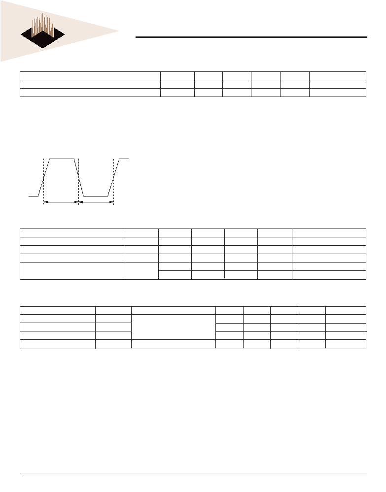
7. Duty cycle is defined as follows.
8. VBS (horizontal sync. component)
9. VBS (vertical sync. component)
10. CLK (input mode)
11. HSY (input mode)
12. VSY (input mode)
13. In case of CLKC=Lo, it shows the phase difference from HSY to
CLK. In that case, HSY will be taken at the rise timing of CLK.
14. In case of CLKC=Lo. it shows the phase difference from VSY to
HSY. In that case, VSY will be taken at the rise timing of HSY.
15. Adjusting the optimal voltage on every module at the typical value
of power supply voltage to get the maximum value of contrast.
However, in the case that the power supply voltage is changed, for
example the level of power supply voltage is reduced, adjust it
externally to get the best contrast with a resistor you add to this
terminal, or semifixed resistor, VCDC, in module. A recommended circuit
is shown in Fig. 5.
TOH
TOL
Duty=TOL/TOH
POWER CONSUMPTION
TA = 25°C
Parameter
SymbolConditions
MIN
TYP
MAX
Unit
Remarks
Positive supply current
ISH
VSH = +8.0V
140
170
mA
Negative supply current
ISL
VSL = -5.0V
55
70
mA
Total
WS
1.4
1.7
W
(16)
Lamp power consumption
WL
normal driving
4.0
W
(17)
16. Excluding backlight section
17. Reference data by calculation (IL x VL x 1: number of lump)
Circuit Diagram
The circuit block diagram of TFT-LCD module is shown
in Fig. 4.
BRT, VCDC, external adjusting recommended circuit is
shown in Fig. 5.
Caution: Turn the power supply on or off (VSH and V SL) at
the same time. Be careful to supply all power voltage
before inputting signals.
Input/Output Signal Waveforms (Fig. 6)
Caution: For the VBS signal, input standard composite
video (or sync.) signal applicable to the operating mode
which have NTSC (M) or PAL (B-G) and is selected by
the NTP signal.
Dimming Backlight by PWM Timing Chart
If using PWM mode, refer to the timing chart shown in
Fig. 7.
相关PDF资料 |
PDF描述 |
|---|---|
| ENH064V1-300 | Low Noise LDO with Low IQ, High PSRR; Temperature Range: -40°C to 85°C; Package: 6-uTDFN T&R |
| ENH064V1-450 | Low Noise LDO with Low IQ, High PSRR; Temperature Range: -40°C to 85°C; Package: 6-uTDFN T&R |
| ENH064V1-600 | 6.4inch VGA |
| ENH064V1-900 | LDO with Low ISUPPLY, High PSRR; Temperature Range: -40°C to 85°C; Package: 8-DFN T&R |
| ENH121S1-250 | LDO with Low ISUPPLY, High PSRR; Temperature Range: -40°C to 85°C; Package: 8-DFN T&R |
相关代理商/技术参数 |
参数描述 |
|---|---|
| ENH057Q1-XXX | 制造商:WEDC 制造商全称:White Electronic Designs Corporation 功能描述:Color TFT-LCD Module Features GENERAL DESCRIPTION |
| ENH-0630 | 制造商:All American Ass'Y 功能描述: |
| ENH064V1-300 | 制造商:WEDC 制造商全称:White Electronic Designs Corporation 功能描述:Color TFT-LCD Module Features |
| ENH064V1-450 | 制造商:WEDC 制造商全称:White Electronic Designs Corporation 功能描述:Color TFT-LCD Module Features |
| ENH064V1-600 | 制造商:WEDC 制造商全称:White Electronic Designs Corporation 功能描述:Color TFT-LCD MODULE FEATURES |
发布紧急采购,3分钟左右您将得到回复。