参数资料
| 型号: | LT1366CS8#TR |
| 厂商: | Linear Technology |
| 文件页数: | 5/20页 |
| 文件大小: | 0K |
| 描述: | IC OPAMP DUAL R-R I/O 8SOIC |
| 标准包装: | 2,500 |
| 放大器类型: | 通用 |
| 电路数: | 2 |
| 输出类型: | 满摆幅 |
| 转换速率: | 0.13 V/µs |
| 增益带宽积: | 400kHz |
| 电流 - 输入偏压: | 10nA |
| 电压 - 输入偏移: | 200µV |
| 电流 - 电源: | 370µA |
| 电流 - 输出 / 通道: | 75mA |
| 电压 - 电源,单路/双路(±): | 1.8 V ~ 30 V,±0.9 V ~ 15 V |
| 工作温度: | 0°C ~ 70°C |
| 安装类型: | 表面贴装 |
| 封装/外壳: | 8-SOIC(0.154",3.90mm 宽) |
| 供应商设备封装: | 8-SO |
| 包装: | 带卷 (TR) |
LT1366/LT1367
LT1368/LT1369
1366fb
applicaTions inForMaTion
Improved Supply Rejection in the LT1368/LT1369
The LT1368/LT1369 are variations of the LT1366/LT1367
offering greater supply rejection and lower high frequency
outputimpedance.TheLT1368/LT1369requirea0.1Fload
capacitance for compensation. The output capacitance
forms a filter, which reduces pickup from the supply and
lowers the output impedance. This additional filtering is
helpfulinmixedanalog/digitalsystemswithcommonsup-
plies, or systems employing switching supplies. Filtering
alsoreduceshighfrequencynoise,whichmaybebeneficial
when driving A/D converters.
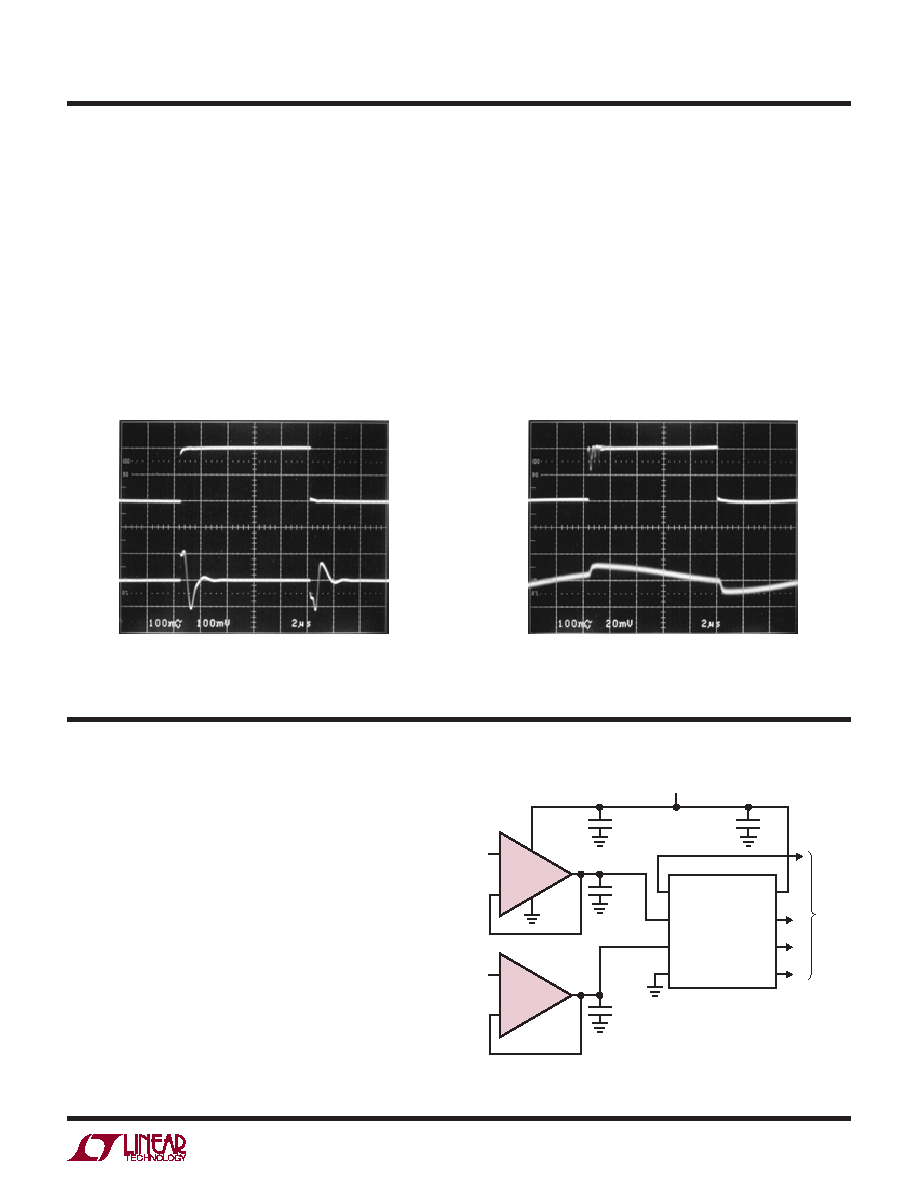
Figure4showstheoutputsoftheLT1366/LT1368perturbed
by a 200mVP-P 50kHz square wave added to the positive
supply. The LT1368’s power supply rejection is about ten
times greater than that of the LT1366 at 50kHz. Note the
5-to-1 scale change in the output voltage traces.
The tolerance of the external compensation capacitor is
not critical. The plots of Overshoot vs Load Current in the
Typical Performance Characteristics section illustrate the
effect of a capacitive load.
2s/DIV
VOUT
100mV/DIV
V+ (AC)
100mV/DIV
LT1366 F04a
2s/DIV
VOUT
20mV/DIV
V+ (AC)
100mV/DIV
LT1366 F04b
Figure 4a. LT1366 Power Supply Rejection Test
Figure 4b. LT1368 Power Supply Rejection Test
Typical applicaTions
Buffering A/D Converters
Figure 5 shows the LT1368 driving an LTC1288 2-chan-
nel micropower A/D converter (ADC). The LTC1288 can
accommodate voltage references and input signals equal
to the supply rails. The sampling nature of this ADC
eliminates the need for an external sample-and-hold, but
may call for a drive amplifier because of the ADC’s 12s
settling requirement. The LT1368’s rail-to-rail operation
and low input offset voltage make it well-suited for low
power, low frequency A/D applications. Either the LT1366
or LT1368 could be used for this application. However,
for low frequencies (f < 1kHz) the LT1368 provides better
supply rejection.
CS/SHDN
CH0
CH1
GND
VCC (REF)
CLK
DOUT
DIN
LTC1288
–
+
–
+
TO P
1F
0.1F
VCC
V0
V1
1/2 LT1368
0.1F
LT1366 FO5
Figure 5. 2-Channel Low Power A/D Converter
相关PDF资料 |
PDF描述 |
|---|---|
| TSW-138-14-G-D | CONN HEADER 76POS .100" DL GOLD |
| LT1352IN8#PBF | IC OP AMP DUAL HI SPD 3MHZ 8-DIP |
| TLW-132-06-G-S | CONN HEADER .100" 32POS SGL GOLD |
| LT1464ACS8#PBF | IC OP-AMP JFET INPUT DUAL 8-SOIC |
| TSW-138-08-G-D | CONN HEADER 76POS .100" DL GOLD |
相关代理商/技术参数 |
参数描述 |
|---|---|
| EPF10K10ATC100-1 | 功能描述:FPGA - 现场可编程门阵列 FPGA - Flex 10K 72 LABs 66 IOs RoHS:否 制造商:Altera Corporation 系列:Cyclone V E 栅极数量: 逻辑块数量:943 内嵌式块RAM - EBR:1956 kbit 输入/输出端数量:128 最大工作频率:800 MHz 工作电源电压:1.1 V 最大工作温度:+ 70 C 安装风格:SMD/SMT 封装 / 箱体:FBGA-256 |
| EPF10K10ATC100-2 | 功能描述:FPGA - 现场可编程门阵列 FPGA - Flex 10K 72 LABs 66 IOs RoHS:否 制造商:Altera Corporation 系列:Cyclone V E 栅极数量: 逻辑块数量:943 内嵌式块RAM - EBR:1956 kbit 输入/输出端数量:128 最大工作频率:800 MHz 工作电源电压:1.1 V 最大工作温度:+ 70 C 安装风格:SMD/SMT 封装 / 箱体:FBGA-256 |
| EPF10K10ATC100-3 | 功能描述:FPGA - 现场可编程门阵列 FPGA - Flex 10K 72 LABs 66 IOs RoHS:否 制造商:Altera Corporation 系列:Cyclone V E 栅极数量: 逻辑块数量:943 内嵌式块RAM - EBR:1956 kbit 输入/输出端数量:128 最大工作频率:800 MHz 工作电源电压:1.1 V 最大工作温度:+ 70 C 安装风格:SMD/SMT 封装 / 箱体:FBGA-256 |
| EPF10K10ATC100-3N | 功能描述:FPGA - 现场可编程门阵列 FPGA - Flex 10K 72 LABs 66 IOs RoHS:否 制造商:Altera Corporation 系列:Cyclone V E 栅极数量: 逻辑块数量:943 内嵌式块RAM - EBR:1956 kbit 输入/输出端数量:128 最大工作频率:800 MHz 工作电源电压:1.1 V 最大工作温度:+ 70 C 安装风格:SMD/SMT 封装 / 箱体:FBGA-256 |
| EPF10K10ATC144-1 | 功能描述:FPGA - 现场可编程门阵列 FPGA - Flex 10K 72 LABs 102 IOs RoHS:否 制造商:Altera Corporation 系列:Cyclone V E 栅极数量: 逻辑块数量:943 内嵌式块RAM - EBR:1956 kbit 输入/输出端数量:128 最大工作频率:800 MHz 工作电源电压:1.1 V 最大工作温度:+ 70 C 安装风格:SMD/SMT 封装 / 箱体:FBGA-256 |
发布紧急采购,3分钟左右您将得到回复。