- 您现在的位置:买卖IC网 > PDF目录43999 > LK1501-9ERD1T 1-OUTPUT 150 W AC-DC REG PWR SUPPLY MODULE PDF资料下载
参数资料
| 型号: | LK1501-9ERD1T |
| 元件分类: | 电源模块 |
| 英文描述: | 1-OUTPUT 150 W AC-DC REG PWR SUPPLY MODULE |
| 封装: | HEAT SINK, METAL, CASE K02, MODULE |
| 文件页数: | 16/27页 |
| 文件大小: | 640K |
| 代理商: | LK1501-9ERD1T |
第1页第2页第3页第4页第5页第6页第7页第8页第9页第10页第11页第12页第13页第14页第15页当前第16页第17页第18页第19页第20页第21页第22页第23页第24页第25页第26页第27页
K-Family
DC-DC Converters >100 W
Rugged Environment
8 - 24
Edition 2/96 - Melcher AG
MELCHER
The Power Partners.
8.1
Formula for the external input capacitor:
2
Po (t h + 0.3 ms) 100
Ci ext = –––––––––––––––––––––– – Ci min
η (U
ti
2 – Ui min2)
where as:
C i min = internal input capacitance [mF]
C i ext = external input capacitance [mF]
Po
= output power [W]
η
= efficiency [%]
t h
= hold-up time [ms]
U i min = minimum input voltage [V] 1
U ti
= threshold level [V]
1 Min. input voltage according to "Electrical Input Data". For out-
put voltages
Uo > Uo nom, the minimum input voltage increases
proportionally to
Uo/Uo nom.
Remarks:
Option V2 and V3 can be adjusted by potentiometer to a
threshold level between
Ui min and Ui max. A decoupling di-
ode should be connected in series with the input of AK...FK
converters to avoid the input capacitance discharging
through other loads connected to the same source voltage.
Option V ACFAIL signal (VME)
This option defines an undervoltage monitoring circuit for
the input or input and main output voltage (
Uo1 nom = 5.1 V
only) equivalent to option D and generates an ACFAIL sig-
nal (V signal) which conforms to the VME standard.
The low state level of the ACFAIL signal is specified at a
sink current of
IV ≤ 48 mA to UV ≤ 0.6 V (open-collector out-
put of a NPN transistor). The pull-up resistor feeding the
open-collector output should be placed on the VME back
plane.
After the ACFAIL signal has gone low, the VME standard
requires a hold-up time
t h of at least 4 ms before the 5.1 V
output drops to 4.875 V when the output is fully loaded.
This hold-up time
t h is provided by the internal input capaci-
tance. Consequently the working input voltage and the
threshold level
U ti should be adequately above the mini-
mum input voltage
Ui min of the converter so that enough
energy is remaining in the input capacitance. If the input
voltage is below the required level, an external hold-up ca-
pacitor (
Ci ext) should be added.
Formula for threshold level for desired value of
th:
2
Po (t h + 0.3 ms) 100
Uti =
––––––––––––––––––––– +
Ui min2
Ci min
η
V output (V0, V2, V3):
Connector pin V is internally connected to the open collec-
tor of a NPN transistor. The emitter is connected to the
negative potential of output 1.
U V ≤ 0.6 V (logic low) corre-
sponds to a monitored voltage level (
Ui and/or Uo1) <Ut.
The current
I V through the open collector should not exceed
50 mA. The NPN output is not protected against external
overvoltages.
U V should not exceed 60 V.
Ui, Uo1 status
V output,
UV
Ui or Uo1 < Ut
low, L,
UV
≤ 0.6 V at IV = 50 mA
Ui and Uo1 > Ut + Uh
high, H,
I V
≤ 25 A at UV = 5.1 V
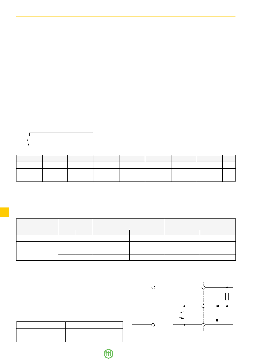
Fig. 28
Output configuration of options V0, V2 and V3
Vo1+
Vo1–
V
UV
IV
Vi+
Vi–
RP
Table 18: Undervoltage monitor functions
V output
Monitoring
Minimum adjustment range
Typical hysteresis
Uh [% of Ut]
(VME compatible)
of threshold level
Ut
for
Ut min…Ut max
Ui
Uo1
Uti
Uto
Uhi
Uho
V2
yes
no
Ui min...Ui max 1–
3.4...0.4
–
V3
yes
Ui min...Ui max 1
0.95...0.985
Uo1 2
3.4...0.4
"0"
V0
yes
no
Ui min...Ui max 3 4
–
3.4...0.4
–
yes
Ui min...Ui max 3 4
0.95...0.985
Uo1 2
3.4...0.4
"0"
1 Threshold level adjustable by potentiometer. 2 Fixed value between 95% and 98 .5% of Uo1 (tracking). 3 Adjusted at Io nom.
4 Fixed value, resistor-adjusted (
±2% at 25°C) acc. to customer's specifications; individual type number is determined by Melcher.
voltage(s) exceed(s)
Ut + Uh. The threshold level Uti is ei-
ther adjustable by potentiometer, accessible through a hole
in the front cover, or adjusted during manufacture to a de-
termined customer specified value.
Versions V0, V2 and V3 are available as shown below.
Option V operates independently of the built-in input under-
voltage lock-out circuit. A logic "low" signal is generated at
pin 20 as soon as one of the monitored voltages drops be-
low the preselected threshold level
Ut. The return for this
signal is Vo1–. The V output recovers when the monitored
Table 17: Available internal input capacitance and factory potentiometer setting of Uti with resulting hold-up time
Types
AK
BK
FK
CK
DK
EK
LK
Unit
Ci min
0.83
0.3
1.2
0.66
0.26
0.21
mF
Ut i
9.5
19.5
39
61
97
120
V DC
th
0.1
3.4
1.1
2.7
4.2
ms
相关PDF资料 |
PDF描述 |
|---|---|
| LK1501-9RD8TB1 | 1-OUTPUT 150 W AC-DC REG PWR SUPPLY MODULE |
| LK1601-9EPD0B1 | 1-OUTPUT 150 W AC-DC REG PWR SUPPLY MODULE |
| LK1601-9EPD2B1 | 1-OUTPUT 150 W AC-DC REG PWR SUPPLY MODULE |
| LK1601-9RD3T | 1-OUTPUT 150 W AC-DC REG PWR SUPPLY MODULE |
| LK1601-9RD6TB1 | 1-OUTPUT 150 W AC-DC REG PWR SUPPLY MODULE |
相关代理商/技术参数 |
参数描述 |
|---|---|
| EPM3512AQC208-10 | 功能描述:CPLD - 复杂可编程逻辑器件 CPLD - MAX 3000A 512 Macro 172 IOs RoHS:否 制造商:Lattice 系列: 存储类型:EEPROM 大电池数量:128 最大工作频率:333 MHz 延迟时间:2.7 ns 可编程输入/输出端数量:64 工作电源电压:3.3 V 最大工作温度:+ 90 C 最小工作温度:0 C 封装 / 箱体:TQFP-100 |
| EPM3512AQC208-10N | 功能描述:CPLD - 复杂可编程逻辑器件 CPLD - MAX 3000A 512 Macro 172 IOs RoHS:否 制造商:Lattice 系列: 存储类型:EEPROM 大电池数量:128 最大工作频率:333 MHz 延迟时间:2.7 ns 可编程输入/输出端数量:64 工作电源电压:3.3 V 最大工作温度:+ 90 C 最小工作温度:0 C 封装 / 箱体:TQFP-100 |
| EPM3512AQC208-7 | 功能描述:CPLD - 复杂可编程逻辑器件 CPLD - MAX 3000A 512 Macro 172 IOs RoHS:否 制造商:Lattice 系列: 存储类型:EEPROM 大电池数量:128 最大工作频率:333 MHz 延迟时间:2.7 ns 可编程输入/输出端数量:64 工作电源电压:3.3 V 最大工作温度:+ 90 C 最小工作温度:0 C 封装 / 箱体:TQFP-100 |
| EPM3512AQC208-7N | 功能描述:CPLD - 复杂可编程逻辑器件 CPLD - MAX 3000A 512 Macro 172 IOs RoHS:否 制造商:Lattice 系列: 存储类型:EEPROM 大电池数量:128 最大工作频率:333 MHz 延迟时间:2.7 ns 可编程输入/输出端数量:64 工作电源电压:3.3 V 最大工作温度:+ 90 C 最小工作温度:0 C 封装 / 箱体:TQFP-100 |
| EPM3512AQI208-10 | 功能描述:CPLD - 复杂可编程逻辑器件 CPLD - MAX 3000A 512 Macro 172 IOs RoHS:否 制造商:Lattice 系列: 存储类型:EEPROM 大电池数量:128 最大工作频率:333 MHz 延迟时间:2.7 ns 可编程输入/输出端数量:64 工作电源电压:3.3 V 最大工作温度:+ 90 C 最小工作温度:0 C 封装 / 箱体:TQFP-100 |
发布紧急采购,3分钟左右您将得到回复。