- 您现在的位置:买卖IC网 > PDF目录17036 > EVAL-AD7262EDZ (Analog Devices Inc)BOARD EVAL CONTROL AD7262 PDF资料下载
参数资料
| 型号: | EVAL-AD7262EDZ |
| 厂商: | Analog Devices Inc |
| 文件页数: | 31/33页 |
| 文件大小: | 0K |
| 描述: | BOARD EVAL CONTROL AD7262 |
| 标准包装: | 1 |
| ADC 的数量: | 2 |
| 位数: | 12 |
| 采样率(每秒): | 1M |
| 数据接口: | 串行 |
| 输入范围: | 5 Vpp |
| 在以下条件下的电源(标准): | 120mW @ 1MSPS |
| 工作温度: | -40°C ~ 105°C |
| 已用 IC / 零件: | AD7262 |
| 已供物品: | 板,CD |
第1页第2页第3页第4页第5页第6页第7页第8页第9页第10页第11页第12页第13页第14页第15页第16页第17页第18页第19页第20页第21页第22页第23页第24页第25页第26页第27页第28页第29页第30页当前第31页第32页第33页
AD7262
Rev. 0 | Page 6 of 32
TIMING SPECIFICATIONS
AVCC = 4.75 V to 5.25 V, CA_CBVCC = CC_CDVCC = 2.7 V to 5.25 V, VREF = 2.5 V internal/external; TA = TMIN to TMAX, unless otherwise noted.1
Table 2.
Limit at TMIN, TMAX
Parameter
2.7 V ≤ VDRIVE ≤ 3.6 V
4.75 V ≤ VDRIVE ≤ 5.25 V
Unit
Description
fSCLK
200
kHz min
40
MHz max
32
MHz typ
20
MHz max
AD7262-5
tCONVERT
19 × tSCLK
ns max
tSCLK = 1/fSCLK
475
ns max
AD7262
950
ns max
AD7262-5
tQUIET
13
ns min
Minimum time between end of serial read/bus relinquish
and next falling edge of CS
t2
10
ns min
CS to SCLK setup time
15
ns max
Delay from 19th SCLK falling edge until DOUTA and DOUTB are
three-state disabled
t4
29
23
ns max
Data access time after SCLK falling edge
t5
15
13
ns min
SCLK to data valid hold time
t6
0.4 × tSCLK
ns min
SCLK high pulse width
t7
0.4 × tSCLK
ns min
SCLK low pulse width
t8
13
ns min
CS rising edge to falling edge pulse width
t9
13
ns max
CS rising edge to DOUTA, DOUTB, high impedance/bus
relinquish
t10
5
ns min
SCLK falling edge to DOUTA, DOUTB, high impedance
35
ns max
SCLK falling edge to DOUTA, DOUTB, high impedance
t11
2
μs min
Minimum CAL pin high time
t12
2
μs min
Minimum time between the CAL pin high and the CS
falling edge
t13
3
ns min
DIN setup time prior to SCLK falling edge
t14
3
ns min
DIN hold time after SCLK falling edge
tPOWER-UP
240
μs max
Internal reference, with a 1 μF decoupling capacitor
15
μs max
With an external reference, 10 μs typical
SCLK
15
19
DOUTA
THREE-STATE
t4
23
4
20
t5
THREE-
STATE
t7
t3
18
DB9A
DB10A
DB11A
21
29
30
31
1 Sample tested during initial release to ensure compliance. All input signals are specified with tR = tF = 5 ns (10% to 90% of AVCC) and timed from a voltage level of 1.6 V.
All timing specifications given are with a 25 pF load capacitance. With a load capacitance greater than this value, a digital buffer or latch must be used. See the
Terminology section.
2 See the Serial Interface section.
3 The time required for the output to cross 0.4 V or 2.4 V.
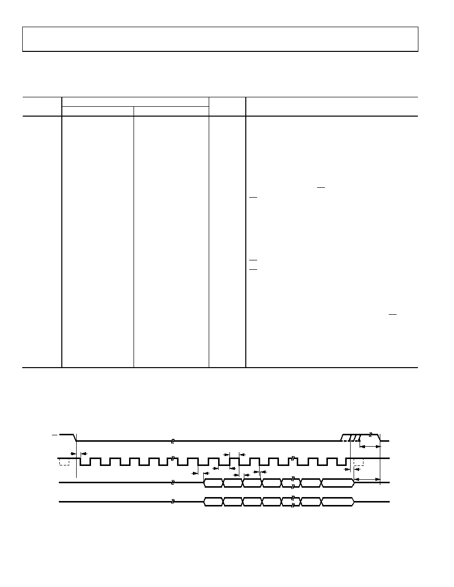
TIMING DIAGRAM
CS
DB1A
DB0A
t2
t9
tQUIET
t8
t6
DOUTB
THREE-STATE
THREE-
STATE
DB9B
DB10B
DB11B
DB1B
DB0B
076
06
-00
2
Figure 2. Serial Interface Timing Diagram
相关PDF资料 |
PDF描述 |
|---|---|
| VE-212-EY | CONVERTER MOD DC/DC 15V 50W |
| EBC20DREH-S734 | CONN EDGECARD 40POS .100 EYELET |
| VE-J1P-EY | CONVERTER MOD DC/DC 13.8V 50W |
| EEC17DRAS-S734 | CONN EDGECARD 34POS .100 R/A PCB |
| VI-J1P-EY | CONVERTER MOD DC/DC 13.8V 50W |
相关代理商/技术参数 |
参数描述 |
|---|---|
| EVAL-AD7264EDZ | 功能描述:BOARD EVALUATION FOR AD7264 RoHS:是 类别:编程器,开发系统 >> 评估板 - 模数转换器 (ADC) 系列:- 产品培训模块:Obsolescence Mitigation Program 标准包装:1 系列:- ADC 的数量:1 位数:12 采样率(每秒):94.4k 数据接口:USB 输入范围:±VREF/2 在以下条件下的电源(标准):- 工作温度:-40°C ~ 85°C 已用 IC / 零件:MAX11645 已供物品:板,软件 |
| EVAL-AD7265CB | 制造商:AD 制造商全称:Analog Devices 功能描述:Differential/Single-Ended Input, Dual 1 MSPS, 12-Bit, 3-Channel SAR ADC |
| EVAL-AD7265CB1 | 制造商:AD 制造商全称:Analog Devices 功能描述:Differential Input, Dual 1 MSPS, 12-Bit, 3-Channel SAR ADC |
| EVAL-AD7265EDZ | 功能描述:BOARD EVAL FOR AD7265 A/D CONV RoHS:是 类别:编程器,开发系统 >> 评估板 - 模数转换器 (ADC) 系列:- 产品培训模块:Obsolescence Mitigation Program 标准包装:1 系列:- ADC 的数量:1 位数:12 采样率(每秒):94.4k 数据接口:USB 输入范围:±VREF/2 在以下条件下的电源(标准):- 工作温度:-40°C ~ 85°C 已用 IC / 零件:MAX11645 已供物品:板,软件 |
| EVAL-AD7266CB | 制造商:Analog Devices 功能描述:EVALUATION CONTROL BOARD I.C. - Bulk |
发布紧急采购,3分钟左右您将得到回复。