- 您现在的位置:买卖IC网 > PDF目录367354 > HY5V26CF-P x16 SDRAM PDF资料下载
参数资料
| 型号: | HY5V26CF-P |
| 英文描述: | x16 SDRAM |
| 中文描述: | x16内存 |
| 文件页数: | 3/14页 |
| 文件大小: | 72K |
| 代理商: | HY5V26CF-P |
HY5V26C(L/S)F
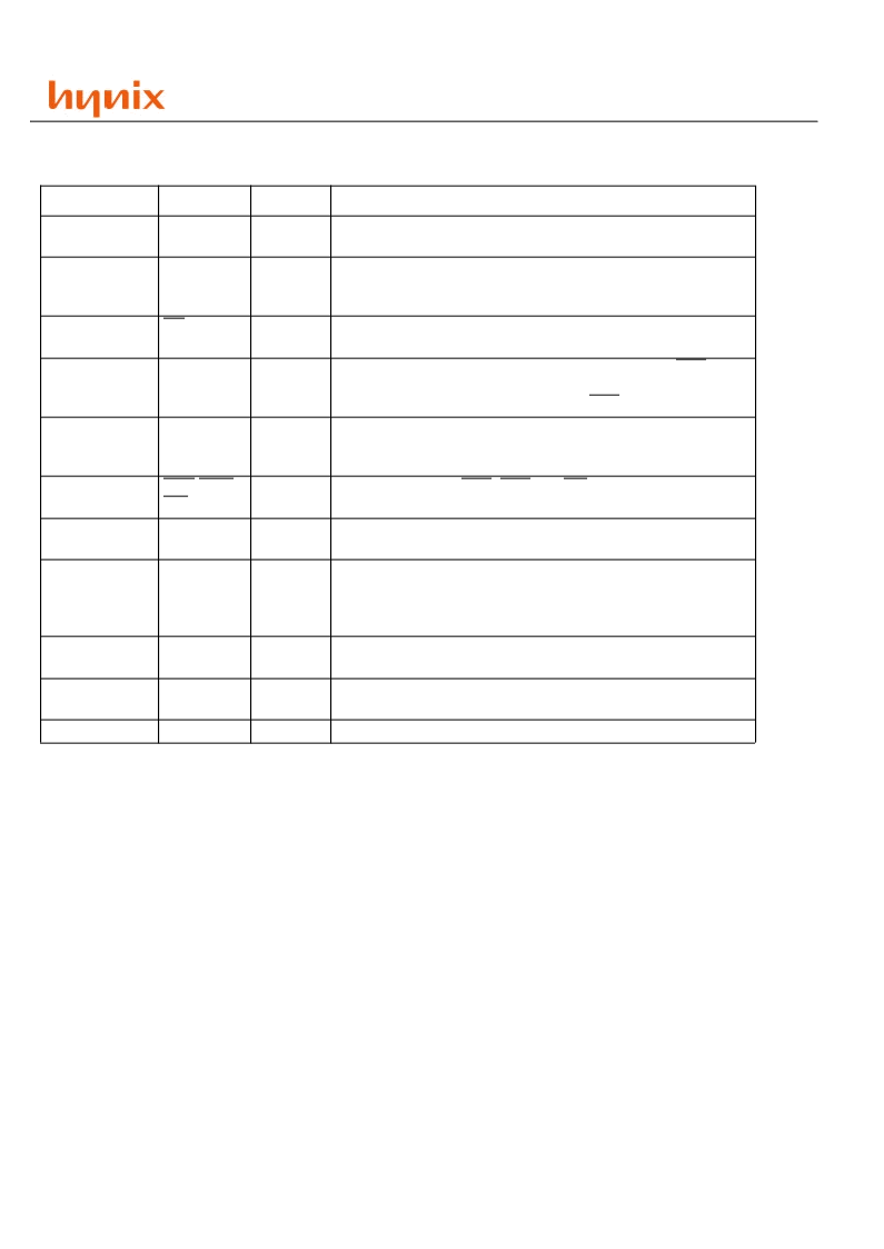
BALL DESCRIPTION
BALL OUT
SYMBOL
TYPE
DESCRIPTION
F2
CLK
INPUT
Clock : The system clock input. All other inputs are registered
to the SDRAM on the rising edge of CLK
Clock Enable : Controls internal clock signal and when deacti-
vated, the SDRAM will be one of the states among power
down, suspend or self refresh
F3
CKE
INPUT
G9
CS
INPUT
Chip Select : Enables or disables all inputs except CLK, CKE,
UDQM and LDQM
Bank Address : Selects bank to be activated during RAS activ-
ity
Selects bank to be read/written during CAS activity
Row Address : RA0 ~ RA11, Column Address : CA0 ~ CA8
Auto-precharge flag : A10
G7,G8
BA0, BA1
INPUT
H7, H8, J8, J7,
J3, J2, H3, H2,
H1, G3, H9, G2
A0 ~ A11
INPUT
F8, F7, F9
RAS, CAS,
WE
UDQM,
LDQM
DQ0 ~
DQ15
INPUT
Command Inputs : RAS, CAS and WE define the operation
Refer function truth table for details
Data Mask:Controls output buffers in read mode and masks
input data in write mode
Data Input/Output:Multiplexed data input/output ball
F1, E8
INPUT
A8, B9, B8, C9,
C8, D9, D8, E9,
E1, D2, D1, C2,
C1, B2, B1, A2
I/O
A9, E7, J9, A1,
E3, J1
A7, B3, C7, D3,
A3, B7, C3, D7
E2, G1
VDD/VSS
SUPPLY
Power supply for internal circuits
VDDQ/
VSSQ
NC
SUPPLY
Power supply for output buffers
-
No connection
相关PDF资料 |
PDF描述 |
|---|---|
| HY5V26CF-PI | x16 SDRAM |
| HY5V26CF-S | x16 SDRAM |
| HY5V26CF-SI | x16 SDRAM |
| HY5V26CLF | 8Mx16|3.3V|4K|6/K/H/8/P/S|SDR SDRAM - 128M |
| HY5V26CLF-6 | x16 SDRAM |
相关代理商/技术参数 |
参数描述 |
|---|---|
| HY5V26CF-PI | 制造商:未知厂家 制造商全称:未知厂家 功能描述:x16 SDRAM |
| HY5V26CF-S | 制造商:未知厂家 制造商全称:未知厂家 功能描述:x16 SDRAM |
| HY5V26CF-SI | 制造商:未知厂家 制造商全称:未知厂家 功能描述:x16 SDRAM |
| HY5V26CLF | 制造商:HYNIX 制造商全称:Hynix Semiconductor 功能描述:4 Banks x 2M x 16bits Synchronous DRAM |
| HY5V26CLF-6 | 制造商:未知厂家 制造商全称:未知厂家 功能描述:x16 SDRAM |
发布紧急采购,3分钟左右您将得到回复。