- 您现在的位置:买卖IC网 > PDF目录67684 > IBM37RGB524CF17A 1600 X 1280 PIXELS PALETTE-DAC DSPL CTLR, PQFP144 PDF资料下载
参数资料
| 型号: | IBM37RGB524CF17A |
| 元件分类: | 显示控制器 |
| 英文描述: | 1600 X 1280 PIXELS PALETTE-DAC DSPL CTLR, PQFP144 |
| 封装: | QFP-144 |
| 文件页数: | 41/72页 |
| 文件大小: | 509K |
| 代理商: | IBM37RGB524CF17A |
第1页第2页第3页第4页第5页第6页第7页第8页第9页第10页第11页第12页第13页第14页第15页第16页第17页第18页第19页第20页第21页第22页第23页第24页第25页第26页第27页第28页第29页第30页第31页第32页第33页第34页第35页第36页第37页第38页第39页第40页当前第41页第42页第43页第44页第45页第46页第47页第48页第49页第50页第51页第52页第53页第54页第55页第56页第57页第58页第59页第60页第61页第62页第63页第64页第65页第66页第67页第68页第69页第70页第71页第72页
40
March 17, 1995
RGB524
IBM
F0-F15: Pixel Frequency 0 to Frequency 15
Index:
0x0020 - 0x002f
Access:
Read/Write
Power on Value: 0x00
Bits 7 - 6
DF - Desired Frequency
Bits 5 - 0
VCO DIV COUNT - VCO Divide
Count
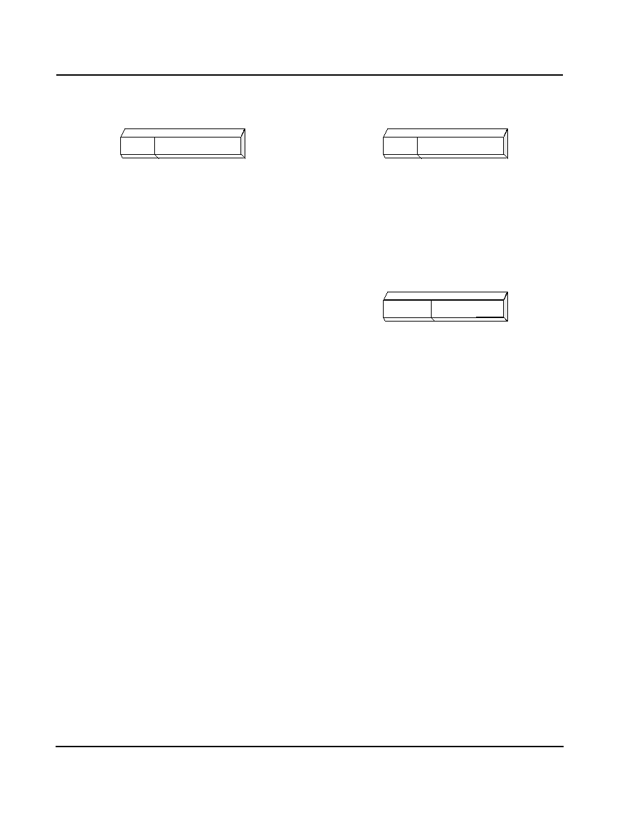
The above register diagram shows the format for the 16
pixel frequency registers F0 - F15. This format is
selected when the EXT/INT bits (Pixel PLL Control 1
register, bits 2:0) = 000 or 010. The selected F0-F15 reg-
ister provides the Pixel PLL with the DF value and the
VCO divide count. All 16 frequency registers work with
the same reference divide count, provided by the Fixed
Pixel PLL Reference Divider register.
These 16 registers have a different format (M, N)
(shown on the following page), when EXT/INT = 001 or
011.
M0-M7, N0-N7
Index:
0x0020, 0x0022, 0x0024, 0x0026,
0x0028, 0x002A, 0x002C, 0x002E
Access:
Read/Write
Power on Value: 0x00
Bits 7 - 6
DF - Desired Frequency
Bits 5 - 0
VCO DIV COUNT - VCO Divide
Count
Index:
0x0021, 0x0023, 0x0025, 0x0027,
0x0029, 0x002B, 0x002D, 0x002F
Access:
Read/Write
Power on Value: 0x00
Bits 7 - 5
Reserved
Bits 4 - 0
REF DIV COUNT - Reference Divide
Count
The above diagrams show the formats for the 8 ‘M’ and 8
“N” pixel frequency registers. These formats are selected
when the EXT/INT bits (Pixel PLL Control 1 Register,
bits 2:0) = 001 or 011.
The 8 registers are grouped into four pairs, M0/N0,
M1/N1, M2/N2, M3/N3. For a given pair, the “M” regis-
ter provides the Pixel PLL with the DF value and the
VCO divide count, and the “N” register provides the
Pixel PLL with the reference divide count.
As described above these 16 registers have a different
format (F) when EXT/INT = 000 or 010.
0
1
2
3
4
5
6
7
DF
VCO DIV COUNT
0
1
2
3
4
5
6
7
DF
VCO DIV COUNT
0
1
2
3
4
5
6
7
Reserved
REF DIV COUNT
相关PDF资料 |
PDF描述 |
|---|---|
| IC-WT-SO16N | ROTARY/LINEAR OPTICAL POSITION ENCODER |
| ICD2028SCR-5 | 100 MHz, PROC SPECIFIC CLOCK GENERATOR, PDSO20 |
| ICD2063SC-1 | 135 MHz, VIDEO CLOCK GENERATOR, PDSO16 |
| ICD2063SC-2 | 135 MHz, VIDEO CLOCK GENERATOR, PDSO16 |
| ICD2063SC-3 | 135 MHz, VIDEO CLOCK GENERATOR, PDSO16 |
相关代理商/技术参数 |
参数描述 |
|---|---|
| IBM37RGB524CF22A | 制造商:未知厂家 制造商全称:未知厂家 功能描述:Video DAC with Color Palette (RAMDAC) |
| IBM39ENV422DLL00C | 制造商:IBM 功能描述: |
| IBM39ENV422PBA17C | 制造商:IBM Microelectronics 功能描述:VID ENCODER 420PIN HPBGA - Trays 制造商:IBM 功能描述:IBM IBM39ENV422PBA17C Encoders - Decoders |
| IBM39MPEGCD20PFD22C | 制造商:IBM 功能描述: |
| IBM39MPEGCS22PFJ22C | 制造商:IBM 功能描述: |
发布紧急采购,3分钟左右您将得到回复。