- 您现在的位置:买卖IC网 > PDF目录377388 > IDT7205S35TP (INTEGRATED DEVICE TECHNOLOGY INC) CMOS ASYNCHRONOUS FIFO 2048 x 9, 4096 x 9, 8192 x 9 and 16384 x 9 PDF资料下载
参数资料
| 型号: | IDT7205S35TP |
| 厂商: | INTEGRATED DEVICE TECHNOLOGY INC |
| 元件分类: | DRAM |
| 英文描述: | CMOS ASYNCHRONOUS FIFO 2048 x 9, 4096 x 9, 8192 x 9 and 16384 x 9 |
| 中文描述: | 8K X 9 OTHER FIFO, 35 ns, PDIP28 |
| 封装: | 0.300 INCH, THIN, PLASTIC, DIP-28 |
| 文件页数: | 6/14页 |
| 文件大小: | 147K |
| 代理商: | IDT7205S35TP |
5.04
6
IDT7203/7204/7205/7206 CMOS ASYNCHRONOUS FIFO
2048 x 9, 4096 x 9, 8192 x 9 and 16384 x 9
MILITARY AND COMMERCIAL TEMPERATURE RANGES
AC TEST CONDITIONS
Input Pulse Levels
Input Rise/Fall Times
Input Timing Reference Levels
Output Reference Levels
Output Load
2661
t
bl 07
CAPACITANCE
(1)
(T
A
= +25
°
C, f = 1.0 MHz)
Symbol
C
IN
(1)
C
OUT
(1,2)
NOTES:
1. This parameter is sampled and not 100% tested.
2. With output deselected.
Parameter
Input Capacitance
Condition
V
IN
= 0V
Max.
10
Unit
pF
Output Capacitance
V
OUT
= 0V
10
pF
2661
t
bl 08
GND to 3.0V
5ns
1.5V
1.5V
See Figure 1
SIGNAL DESCRIPTIONS
Inputs:
DATA IN (D
0
–D
8
)
— Data inputs for 9-bit wide data.
Controls:
RESET (
(
RS
) input is taken to a LOW state. During reset, both internal
read and write pointers are set to the first location. A reset is
required after power-up before a write operation can take place.
Both the Read Enable (
R
) and Write Enable (
W
) inputs must
be in the HIGH state during the window shown in Figure 2
(i.e. t
RSS
before the rising edge of
change until t
RSR
after the rising edge of
RS
) —
Reset is accomplished whenever the Reset
RS
) and should not
RS
.
WRITE ENABLE (
W
) —
A write cycle is initiated on the falling
edge of this input if the Full Flag (
FF
) is not set. Data set-up and
hold times must be adhered-to, with respect to the rising edge
of the Write Enable (
W
). Data is stored in the RAM array
sequentially and independently of any on-going read operation.
After half of the memory is filled, and at the falling edge of the
next write operation, the Half-Full Flag (
HF
) will be set to LOW,
and will remain set until the difference between the write pointer
and read pointer is less-than or equal to one-half of the total
memory of the device. The Half-Full Flag (
HF
) is reset by the
rising edge of the read operation.
To prevent data overflow, the Full Flag (
FF
) will go LOW on
the falling edge of the last write signal, which inhibits further write
operations. Upon the completion of a valid read operation, the
Full Flag (
FF
) will go HIGH after t
RFF
, allowing a new valid write
to begin. When the FIFO is full, the internal write pointer is
blocked from
W
, so external changes in
W
will not affect the FIFO
when it is full.
READ ENABLE (
R
) —
A read cycle is initiated on the falling
edge of the Read Enable (
R
), provided the Empty Flag (
EF
) is not
set. The data is accessed on a First-In/First-Out basis, inde-
pendent of any ongoing write operations. After Read Enable (
R
)
goes HIGH, the Data Outputs (Q
0
through Q
8
) will return to a
high-impedance condition until the next Read operation. When
all the data has been read from the FIFO, the Empty Flag (
EF
)
will go LOW, allowing the “final” read cycle but inhibiting further
read operations, with the data outputs remaining in a high-
impedance state. Once a valid write operation has been accom-
plished, the Empty Flag (
EF
) will go HIGH after t
WEF
and a valid
Read can then begin. When the FIFO is empty, the internal read
pointer is blocked from
R
so external changes will not affect the
FIFO when it is empty.
FIRST LOAD/RETRANSMIT (
FL
purpose input. In the Depth Expansion Mode, this pin is
grounded to indicate that it is the first device loaded (see
Operating Modes). The Single Device Mode is initiated by
grounding the Expansion In (
XI
).
The IDT7203/7204/7205/7206 can be made to retransmit
data when the Retransmit Enable Control (
RT
) input is pulsed
LOW. A retransmit operation will set the internal read pointer to
the first location and will not affect the write pointer. The status
of the Flags will change depending on the relative locations of
the read and write pointers. Read Enable (
R
) and Write Enable
(
W
) must be in the HIGH state during retransmit. This feature is
useful when less than 2048/4096/8192/16384 writes are per-
formed between resets. The retransmit feature is not compat-
ible with the Depth Expansion Mode.
/
RT
) —
This is a dual-
EXPANSION IN (
XI
)
— This input is a dual-purpose pin.
Expansion In (
XI
) is grounded to indicate an operation in the
single device mode. Expansion In (
XI
) is connected to Expan-
sion Out (
XO
) of the previous device in the Depth Expansion or
Daisy-Chain Mode.
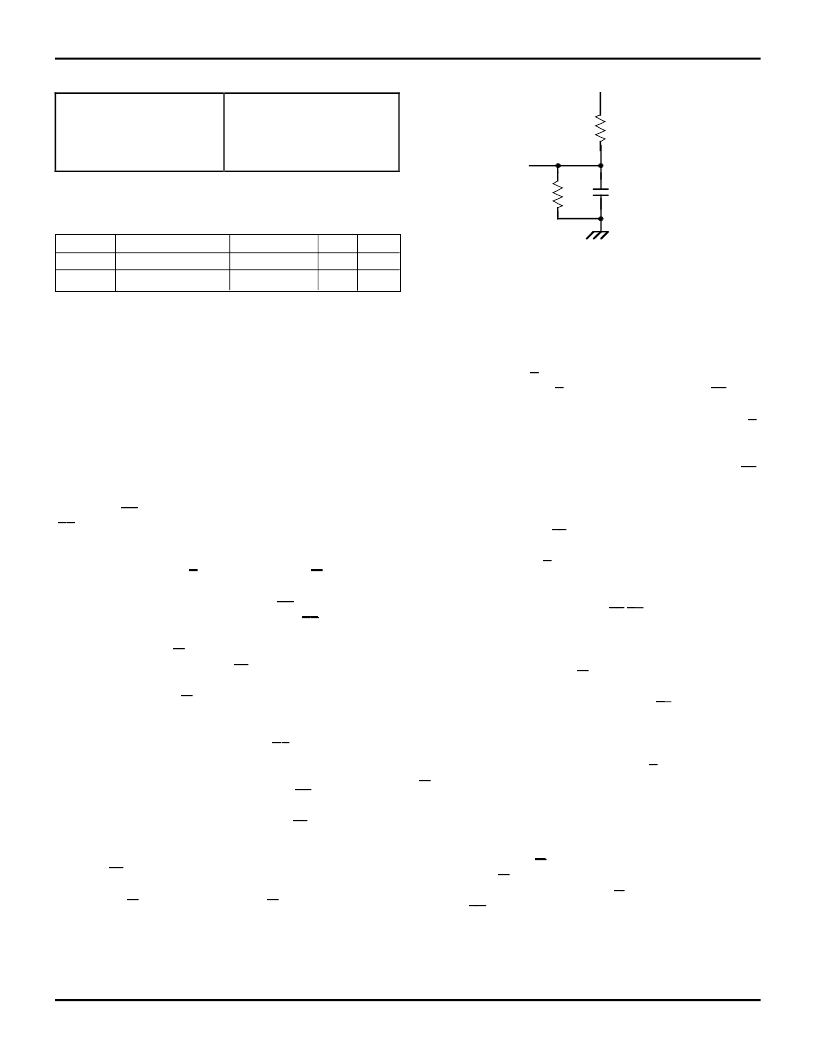
1.1K
30pF*
680
5V
D.U.T.
OR EQUIVALENT CIRCUIT
2661 drw 03
Figure 1. Output Load
*Includes jig and scope capacitances.
相关PDF资料 |
PDF描述 |
|---|---|
| IDT7205S35TPB | CMOS ASYNCHRONOUS FIFO 2048 x 9, 4096 x 9, 8192 x 9 and 16384 x 9 |
| IDT7205S50D | CMOS ASYNCHRONOUS FIFO 2048 x 9, 4096 x 9, 8192 x 9 and 16384 x 9 |
| IDT7205S50DB | CMOS ASYNCHRONOUS FIFO 2048 x 9, 4096 x 9, 8192 x 9 and 16384 x 9 |
| IDT7205S50J | CMOS ASYNCHRONOUS FIFO 2048 x 9, 4096 x 9, 8192 x 9 and 16384 x 9 |
| IDT7205S50JB | CMOS ASYNCHRONOUS FIFO 2048 x 9, 4096 x 9, 8192 x 9 and 16384 x 9 |
相关代理商/技术参数 |
参数描述 |
|---|---|
| IDT7206L15J | 功能描述:IC FIFO 8192X18 15NS 32PLCC RoHS:否 类别:集成电路 (IC) >> 逻辑 - FIFO 系列:7200 标准包装:90 系列:74ABT 功能:同步,双端口 存储容量:4.6K(64 x 36 x2) 数据速率:67MHz 访问时间:- 电源电压:4.5 V ~ 5.5 V 工作温度:0°C ~ 70°C 安装类型:表面贴装 封装/外壳:120-LQFP 裸露焊盘 供应商设备封装:120-HLQFP(14x14) 包装:托盘 产品目录页面:1005 (CN2011-ZH PDF) 其它名称:296-3984 |
| IDT7206L15J8 | 功能描述:IC FIFO 8192X18 15NS 32PLCC RoHS:否 类别:集成电路 (IC) >> 逻辑 - FIFO 系列:7200 标准包装:90 系列:7200 功能:同步 存储容量:288K(16K x 18) 数据速率:100MHz 访问时间:10ns 电源电压:4.5 V ~ 5.5 V 工作温度:0°C ~ 70°C 安装类型:表面贴装 封装/外壳:64-LQFP 供应商设备封装:64-TQFP(14x14) 包装:托盘 其它名称:72271LA10PF |
| IDT7206L15JG | 功能描述:IC FIFO 8192X18 15NS 32PLCC RoHS:是 类别:集成电路 (IC) >> 逻辑 - FIFO 系列:7200 标准包装:90 系列:7200 功能:同步 存储容量:288K(16K x 18) 数据速率:100MHz 访问时间:10ns 电源电压:4.5 V ~ 5.5 V 工作温度:0°C ~ 70°C 安装类型:表面贴装 封装/外壳:64-LQFP 供应商设备封装:64-TQFP(14x14) 包装:托盘 其它名称:72271LA10PF |
| IDT7206L15JG8 | 功能描述:IC FIFO 8192X18 15NS 32PLCC RoHS:是 类别:集成电路 (IC) >> 逻辑 - FIFO 系列:7200 标准包装:90 系列:7200 功能:同步 存储容量:288K(16K x 18) 数据速率:100MHz 访问时间:10ns 电源电压:4.5 V ~ 5.5 V 工作温度:0°C ~ 70°C 安装类型:表面贴装 封装/外壳:64-LQFP 供应商设备封装:64-TQFP(14x14) 包装:托盘 其它名称:72271LA10PF |
| IDT7206L15P | 功能描述:IC FIFO 8192X18 15NS 28DIP RoHS:否 类别:集成电路 (IC) >> 逻辑 - FIFO 系列:7200 标准包装:90 系列:7200 功能:同步 存储容量:288K(16K x 18) 数据速率:100MHz 访问时间:10ns 电源电压:4.5 V ~ 5.5 V 工作温度:0°C ~ 70°C 安装类型:表面贴装 封装/外壳:64-LQFP 供应商设备封装:64-TQFP(14x14) 包装:托盘 其它名称:72271LA10PF |
发布紧急采购,3分钟左右您将得到回复。