- 您现在的位置:买卖IC网 > PDF目录377488 > IDT82V3002APV (INTEGRATED DEVICE TECHNOLOGY INC) WAN PLL WITH DUAL REFERENCE INPUTS PDF资料下载
参数资料
| 型号: | IDT82V3002APV |
| 厂商: | INTEGRATED DEVICE TECHNOLOGY INC |
| 元件分类: | 通信及网络 |
| 英文描述: | WAN PLL WITH DUAL REFERENCE INPUTS |
| 中文描述: | SPECIALTY TELECOM CIRCUIT, PDSO56 |
| 封装: | SSOP-56 |
| 文件页数: | 16/28页 |
| 文件大小: | 390K |
| 代理商: | IDT82V3002APV |
第1页第2页第3页第4页第5页第6页第7页第8页第9页第10页第11页第12页第13页第14页第15页当前第16页第17页第18页第19页第20页第21页第22页第23页第24页第25页第26页第27页第28页
16
IDT82V3002A WAN PLL WITH DUAL REFERENCE INPUTS INDUSTRIAL TEMPERATURE RANGE
24.704 MHz for C6, E1 and T1 divider respectively.
In Holdover mode, the DCO is running at the same frequency which
is generated by using the storage techniques.
In Freerun mode, the DCO is running at the same frequency as that
of the master clock.
3.7.6
LOCK INDICATOR
In Normal Mode, the LOCK pin will be set to high only when the
following equation is satisfied:
|f
out
– f
in
|
≤
0.4 ppm
f
out
= the average frequency of the output clock signal from the DPLL
(within 2 seconds)
f
in
= the average frequency of the input reference (within 2 seconds)
In other operation modes, the LOCK pin remains low.
3.7.7
OUTPUT INTERFACE
The Output Interface uses three output signals of the DCO to
generate eight types of clock signals and six types of framing signals
totally.
The 32.768 MHz signal is used by the E1_divider to generate five
types of clock signals (C2o,
C4o
, C8o,
C16o
and
C32o
) with nominal
50% duty cycle and six types of framing signals (F0o, F8o,
F16o
,
F32o
,
RSP and TSP).
The 24.704 MHz signal is used by the T1_divider to generate two
types of T1 signals (C1.5o and
C3o
) with nominal 50% duty cycle.
The 25.248 MHz signal is used by the C6_divider to generate a C6o
signal with nominal 50% duty cycle.
All these output signals are synchronous to F8o.
3.8
OSC
The IDT82V3002A can use a clock as the master timing source.
In Freerun Mode, the frequency tolerance at the clock outputs is
identical to that of the source at the OSCi pin. For applications not
requiring an accurate Freerun Mode, the tolerance of the master timing
source may be ±100 ppm. For applications requiring an accurate
Freerun Mode, such as AT&T TR62411, the tolerance of the master
timing source must be no greater than ±32 ppm.
The desired capture range should be taken into consideration when
determining the accuracy of the master timing source. The sum of the
accuracy of the master timing source and the capture range of the
IDT82V3002A will always equal 230 ppm. For example, if the master
timing source is 100 ppm, the capture range will be 130 ppm.
3.8.1
CLOCK OSCILLATOR
When selecting a clock oscillator, numerous parameters must be
considered, including absolute frequency, frequency change over
temperature, output rise and fall times, output levels and duty cycle.
For applications requiring ±32 ppm clock accuracy, the following
clock oscillator module may be used.
FOX F7C-2E3-20.0 MHz
Frequency:
20 MHz
Tolerance:
25 ppm 0°C to 70°C
Rise & Fall Time:10 ns (0.33 V 2.97 V 15 pF)
Duty Cycle:
40% to 60%
The output clock should be connected directly (not AC coupled) to
the OSCi input of the IDT82V3002A, and the OSCo output should be left
open as shown in
Figure - 9
.
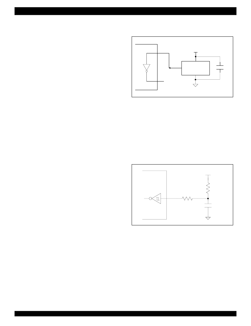
Figure - 9 Clock Oscillator Circuit
3.9
JTAG
The IDT82V3002A supports IEEE 1149.1 JTAG Scan.
3.10
RESET CIRCUIT
A simple power up reset circuit is shown in
Figure - 10
. Resistor Rp is
used for protection only and limits current into the
RST
pin during power
down conditions. The reset low time is not critical but should be greater
than 300 ns. In
Figure - 10
,
the reset low time is about 50 μs.
Figure - 10 Power-Up Reset Circuit
+3.3 V
20 MHz OUT
GND
+3.3 V
No Connection
OSCo
OSCi
IDT82V3002A
0.1
μ
F
3.3 V
R
10 k
Rp
1 k
C
1
μ
F
RST
IDT82V3002A
相关PDF资料 |
PDF描述 |
|---|---|
| IDT82V3010 | T1/E1/OC3 TELECOM CLOCK GENERATOR WITH DUAL REFERENCE INPUTS |
| IDT82V3010PV | T1/E1/OC3 TELECOM CLOCK GENERATOR WITH DUAL REFERENCE INPUTS |
| IDT82V3010PVG | T1/E1/OC3 TELECOM CLOCK GENERATOR WITH DUAL REFERENCE INPUTS |
| IDT82V3255 | WAN PLL |
| IDT82V3255DK | WAN PLL |
相关代理商/技术参数 |
参数描述 |
|---|---|
| IDT82V3002APVG | 功能描述:IC PLL WAN T1/E1 DUAL REF 56SSOP RoHS:是 类别:集成电路 (IC) >> 时钟/计时 - 专用 系列:- 标准包装:1,500 系列:- 类型:时钟缓冲器/驱动器 PLL:是 主要目的:- 输入:- 输出:- 电路数:- 比率 - 输入:输出:- 差分 - 输入:输出:- 频率 - 最大:- 电源电压:3.3V 工作温度:0°C ~ 70°C 安装类型:表面贴装 封装/外壳:28-SSOP(0.209",5.30mm 宽) 供应商设备封装:28-SSOP 包装:带卷 (TR) 其它名称:93786AFT |
| IDT82V3002APVG8 | 功能描述:IC PLL WAN T1/E1 DUAL REF 56SSOP RoHS:是 类别:集成电路 (IC) >> 时钟/计时 - 专用 系列:- 标准包装:1,500 系列:- 类型:时钟缓冲器/驱动器 PLL:是 主要目的:- 输入:- 输出:- 电路数:- 比率 - 输入:输出:- 差分 - 输入:输出:- 频率 - 最大:- 电源电压:3.3V 工作温度:0°C ~ 70°C 安装类型:表面贴装 封装/外壳:28-SSOP(0.209",5.30mm 宽) 供应商设备封装:28-SSOP 包装:带卷 (TR) 其它名称:93786AFT |
| IDT82V3010 | 制造商:IDT 制造商全称:Integrated Device Technology 功能描述:T1/E1/OC3 TELECOM CLOCK GENERATOR WITH DUAL REFERENCE INPUTS |
| IDT82V3010PV | 制造商:IDT 制造商全称:Integrated Device Technology 功能描述:T1/E1/OC3 TELECOM CLOCK GENERATOR WITH DUAL REFERENCE INPUTS |
| IDT82V3010PVG | 功能描述:IC PLL WAN 51/E1/OC3 DUAL 56SSOP RoHS:是 类别:集成电路 (IC) >> 时钟/计时 - 专用 系列:- 标准包装:1,500 系列:- 类型:时钟缓冲器/驱动器 PLL:是 主要目的:- 输入:- 输出:- 电路数:- 比率 - 输入:输出:- 差分 - 输入:输出:- 频率 - 最大:- 电源电压:3.3V 工作温度:0°C ~ 70°C 安装类型:表面贴装 封装/外壳:28-SSOP(0.209",5.30mm 宽) 供应商设备封装:28-SSOP 包装:带卷 (TR) 其它名称:93786AFT |
发布紧急采购,3分钟左右您将得到回复。