- 您现在的位置:买卖IC网 > PDF目录377488 > IDT82V3002APV (INTEGRATED DEVICE TECHNOLOGY INC) WAN PLL WITH DUAL REFERENCE INPUTS PDF资料下载
参数资料
| 型号: | IDT82V3002APV |
| 厂商: | INTEGRATED DEVICE TECHNOLOGY INC |
| 元件分类: | 通信及网络 |
| 英文描述: | WAN PLL WITH DUAL REFERENCE INPUTS |
| 中文描述: | SPECIALTY TELECOM CIRCUIT, PDSO56 |
| 封装: | SSOP-56 |
| 文件页数: | 7/28页 |
| 文件大小: | 390K |
| 代理商: | IDT82V3002APV |
第1页第2页第3页第4页第5页第6页当前第7页第8页第9页第10页第11页第12页第13页第14页第15页第16页第17页第18页第19页第20页第21页第22页第23页第24页第25页第26页第27页第28页
7
IDT82V3002A WAN PLL WITH DUAL REFERENCE INPUTS INDUSTRIAL TEMPERATURE RANGE
2
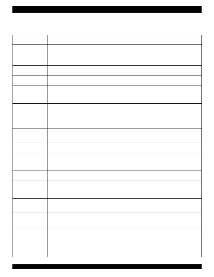
PIN DESCRIPTION
Table - 1 Pin Description
Name
Type
Pin
Number
Description
V
SS
Power
12, 18, 27,
38, 47
Ground.
0 V. All V
SS
pins should be connected to the ground.
V
DD
Power
13, 19, 26,
37, 48
Positive Supply Voltage.
All V
DD
pins should be connected to +3.3 V nominal.
OSCo
(CMOS) O
49
Oscillator Master Clock.
This pin is left unconnected.
OSCi
(CMOS) I
50
Oscillator Master Clock.
This pin is connected to a clock source.
Fref0
I
5
Reference Input 0.
This is one of the input reference sources (falling edge) used for synchronization. One of three possible frequencies (8
kHz, 1.544 MHz, or 2.048 MHz) may be used. The selection of the input reference is determined by IN_sel control input.
See
Table - 4
. This pin is internally pulled up to V
DD
.
Fref1
I
6
Reference Input 1.
See above. This pin is internally pulled up to V
DD
.
IN_sel
I
11
Reference Switch Input Control.
A logic low selects Reference Input 0 (Fref0) and a logic high selects Reference Input 1 (Fref1). The logic level at this
input is gated in by the rising edge of F8o. This pin is internally pulled down to V
SS
.
F_sel1
I
10
Input Frequency Select 1.
This input, in conjunction with F_sel0, determines which of three possible frequencies (8 kHz, 1.544 MHz, or 2.048 MHz )
may be input to the Reference Input 0 and Reference Input 1. See
Table - 3
.
F_sel0
I
9
Input Frequency Select 0.
See above.
MODE_sel1
I
2
Mode/Control Select 1.
This input, in conjunction with MODE_sel0, determines the operation mode of the IDT82V3002A (Normal, Holdover or
Freerun). The logic level at this input is gated in by the rising edge of F8o. This pin is internally pulled down to V
SS
. See
Table - 2
.
MODE_sel0
I
1
Mode/Control Select 0.
See above. The logic level at this input is gated in by the rising edge of F8o. This pin is internally pulled down to V
SS
.
RST
I
4
Reset Input.
A logic low at this pin resets the IDT82V3002A. To ensure proper operation, the device must be reset after the frequency
of the input reference is changed and power-up. The
RST
pin should be held low for a minimum of 300 ns. While the
RST
pin is low, all framing and clock outputs are at logic high.
TCLR
I
3
TIE Circuit Reset.
Logic low at this input resets the TIE (Time Interval Error) control block, resulting in a realignment of output phase with
input phase. The
TCLR
pin should be held low for a minimum of 300 ns. This pin is internally pulled up to V
DD
.
TIE_en
I
56
TIE Enable.
A logic high at this pin enables the TIE control block while a logic low at this pin disables the TIE control block. The logic
level at this input is gated in by the rising edge of F8o. This pin is internally pulled down to V
ss
.
FLOCK
I
45
Fast Lock Mode.
Set high to allow the DPLL to quickly lock to the input reference (less than 500 ms locking time).
LOCK
(CMOS) O
44
Lock Indicator.
This output goes high when the DPLL is frequency locked to the input reference.
HOLDOVER (CMOS) O
52
Holdover Indicator.
This output goes to a logic high whenever the DPLL goes into Holdover Mode.
相关PDF资料 |
PDF描述 |
|---|---|
| IDT82V3010 | T1/E1/OC3 TELECOM CLOCK GENERATOR WITH DUAL REFERENCE INPUTS |
| IDT82V3010PV | T1/E1/OC3 TELECOM CLOCK GENERATOR WITH DUAL REFERENCE INPUTS |
| IDT82V3010PVG | T1/E1/OC3 TELECOM CLOCK GENERATOR WITH DUAL REFERENCE INPUTS |
| IDT82V3255 | WAN PLL |
| IDT82V3255DK | WAN PLL |
相关代理商/技术参数 |
参数描述 |
|---|---|
| IDT82V3002APVG | 功能描述:IC PLL WAN T1/E1 DUAL REF 56SSOP RoHS:是 类别:集成电路 (IC) >> 时钟/计时 - 专用 系列:- 标准包装:1,500 系列:- 类型:时钟缓冲器/驱动器 PLL:是 主要目的:- 输入:- 输出:- 电路数:- 比率 - 输入:输出:- 差分 - 输入:输出:- 频率 - 最大:- 电源电压:3.3V 工作温度:0°C ~ 70°C 安装类型:表面贴装 封装/外壳:28-SSOP(0.209",5.30mm 宽) 供应商设备封装:28-SSOP 包装:带卷 (TR) 其它名称:93786AFT |
| IDT82V3002APVG8 | 功能描述:IC PLL WAN T1/E1 DUAL REF 56SSOP RoHS:是 类别:集成电路 (IC) >> 时钟/计时 - 专用 系列:- 标准包装:1,500 系列:- 类型:时钟缓冲器/驱动器 PLL:是 主要目的:- 输入:- 输出:- 电路数:- 比率 - 输入:输出:- 差分 - 输入:输出:- 频率 - 最大:- 电源电压:3.3V 工作温度:0°C ~ 70°C 安装类型:表面贴装 封装/外壳:28-SSOP(0.209",5.30mm 宽) 供应商设备封装:28-SSOP 包装:带卷 (TR) 其它名称:93786AFT |
| IDT82V3010 | 制造商:IDT 制造商全称:Integrated Device Technology 功能描述:T1/E1/OC3 TELECOM CLOCK GENERATOR WITH DUAL REFERENCE INPUTS |
| IDT82V3010PV | 制造商:IDT 制造商全称:Integrated Device Technology 功能描述:T1/E1/OC3 TELECOM CLOCK GENERATOR WITH DUAL REFERENCE INPUTS |
| IDT82V3010PVG | 功能描述:IC PLL WAN 51/E1/OC3 DUAL 56SSOP RoHS:是 类别:集成电路 (IC) >> 时钟/计时 - 专用 系列:- 标准包装:1,500 系列:- 类型:时钟缓冲器/驱动器 PLL:是 主要目的:- 输入:- 输出:- 电路数:- 比率 - 输入:输出:- 差分 - 输入:输出:- 频率 - 最大:- 电源电压:3.3V 工作温度:0°C ~ 70°C 安装类型:表面贴装 封装/外壳:28-SSOP(0.209",5.30mm 宽) 供应商设备封装:28-SSOP 包装:带卷 (TR) 其它名称:93786AFT |
发布紧急采购,3分钟左右您将得到回复。