- 您现在的位置:买卖IC网 > PDF目录65596 > IL1208AT-X001 (VISHAY SEMICONDUCTORS) 1 CHANNEL TRANSISTOR OUTPUT OPTOCOUPLER PDF资料下载
参数资料
| 型号: | IL1208AT-X001 |
| 厂商: | VISHAY SEMICONDUCTORS |
| 元件分类: | 光电耦合器 |
| 英文描述: | 1 CHANNEL TRANSISTOR OUTPUT OPTOCOUPLER |
| 封装: | LEAD FREE, SMD, SOIC-8 |
| 文件页数: | 2/9页 |
| 文件大小: | 159K |
| 代理商: | IL1208AT-X001 |
www.vishay.com
For technical questions, contact: optocoupler.answers@vishay.com
Document Number: 83549
302
Rev. 1.7, 08-May-08
IL1205AT/1206AT/1207AT/1208AT
Vishay Semiconductors Optocoupler, Phototransistor Output,
with Base Connection in SOIC-8
Package, 110 °C Rated
Notes
(1) Tamb = 25 °C, unless otherwise specified.
Stresses in excess of the absolute maximum ratings can cause permanent damage to the device. Functional operation of the device is not
implied at these or any other conditions in excess of those given in the operational sections of this document. Exposure to absolute maximum
ratings for extended periods of the time can adversely affect reliability.
(2) Refer to reflow profile for soldering conditions for surface mounted devices (SOP/SOIC).
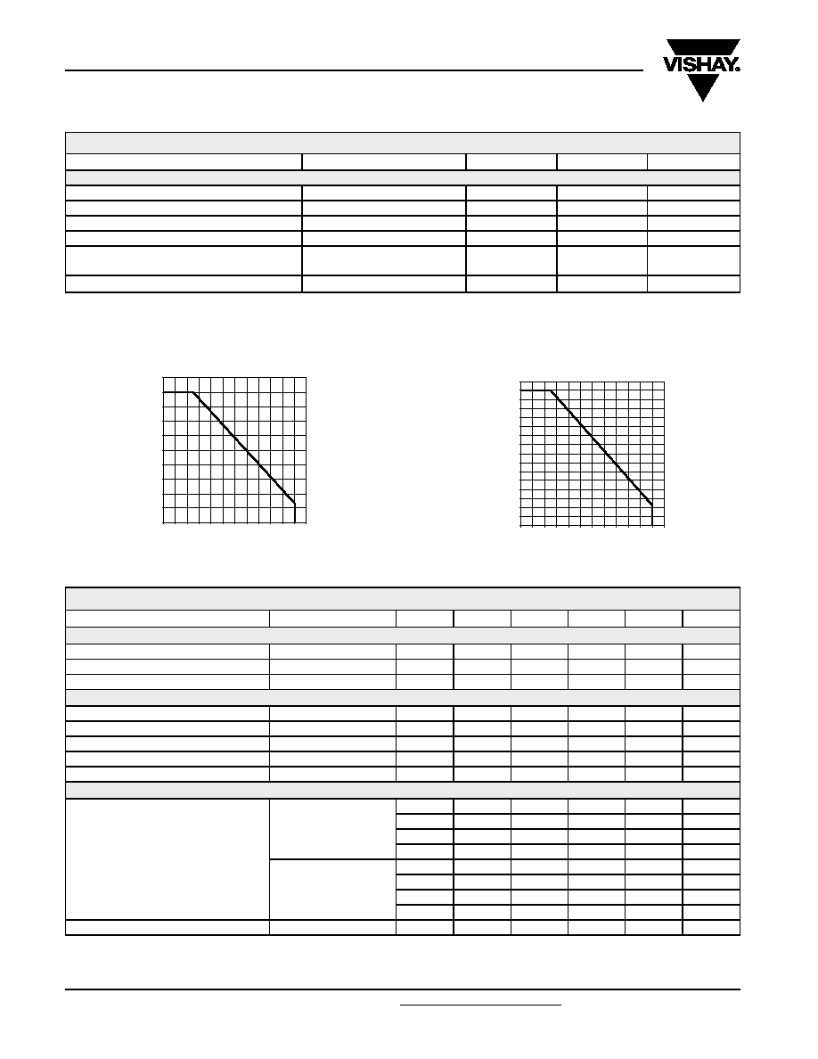
Fig. 1 - Input Power Dissipation (LED) vs. Ambient Temperature
Fig. 2 - Output Power Dissipation vs. Ambient Temperature
Note
Tamb = 25 °C, unless otherwise specified.
Minimum and maximum values were tested requierements. Typical values are characteristics of the device and are the result of engineering
evaluations. Typical values are for information only and are not part of the testing requirements.
COUPLER
Isolation test voltage
VISO
4000
VRMS
Operating temperature
Tamb
- 55 to + 110
°C
Total package dissipation (LED and detector)
Ptot
240
mW
Storage temperature
Tstg
- 55 to + 150
°C
Soldering temperature (2)
max. 10 s, dip soldering distance
to seating plane
≥ 1.5 mm
Tsld
260
°C
Derate linearly from 25 °C
2.4
mW/°C
ABSOLUTE MAXIMUM RATINGS (1)
PARAMETER
TEST CONDITION
SYMBOL
VALUE
UNIT
010 20 30 4050 60 70 80 90 100 110 120
0
10
20
30
40
50
60
70
80
90
100
Tamb (°C)
LED
P
o
w
er
P
diss
(m
W
)
0 10 20 30 40 50 60 70 80 90 100110 120
0
10
20
30
40
50
60
70
80
90
100
Tamb (°C)
O
u
tp
u
tP
o
w
er
P
diss
(m
W
)
110
120
130
140
150
160
ELECTRICAL CHARACTERISTCS
PARAMETER
TEST CONDITION
PART
SYMBOL
MIN.
TYP.
MAX.
UNIT
INPUT
Forward voltage
IF = 10 mA
VF
1.3
1.5
V
Reverse current
VR = 6 V
IR
0.1
100
A
Capacitance
VR = 0 V
CI
13
pF
OUTPUT
Collector emitter leakage current
VCE = 10 V
ICEO
5.0
50
nA
Collector emitter breakdown voltage
IC = 100 A
BVCEO
70
V
Emitter collector breakdown voltage
IE = 100 A
BVECO
7.0
10
V
Collector base breakdown current
BVCBO
70
V
Saturation voltage, collector emitter
IC = 2 mA, IF = 10 mA
VCEsat
0.4
V
COUPLER
DC current transfer ratio
IF = 10 mA, VCE = 5.0 V
IL1205AT
CTR
40
80
%
IL1206AT
CTR
63
125
%
IL1207AT
CTR
100
200
%
IL1208AT
CTR
100
320
%
IF = 1.0 mA, VCE = 5.0 V
IL1205AT
CTR
13
25
%
IL1206AT
CTR
22
40
%
IL1207AT
CTR
34
60
%
IL1208AT
CTR
56
95
%
Capacitance (input to output)
CIO
0.5
pF
相关PDF资料 |
PDF描述 |
|---|---|
| IL1206AT-X001 | 1 CHANNEL TRANSISTOR OUTPUT OPTOCOUPLER |
| IL1207AT-X001 | 1 CHANNEL TRANSISTOR OUTPUT OPTOCOUPLER |
| IL203-X001 | 1 CHANNEL TRANSISTOR OUTPUT OPTOCOUPLER |
| IL201-X001 | 1 CHANNEL TRANSISTOR OUTPUT OPTOCOUPLER |
| IL202 | 1 CHANNEL TRANSISTOR OUTPUT OPTOCOUPLER |
相关代理商/技术参数 |
参数描述 |
|---|---|
| IL1209 | 制造商:未知厂家 制造商全称:未知厂家 功能描述:DC to DC Converter |
| IL1209H | 制造商:未知厂家 制造商全称:未知厂家 功能描述:DC to DC Converter |
| IL1209S | 制造商:XP Power 功能描述:CONVERTER DC/DC 2W 9V 制造商:XP Power 功能描述:CONVERTER, DC/DC, 2W, 9V 制造商:XP Power 功能描述:DC-DC CONV, ISO POL, 1 O/P, 2W, 222mA, 9V; DC / DC Converter Type:Isolated POL; DC / DC Converter Output Type:Fixed; Input Voltage DC Min:10.8V; Input Voltage DC Max:13.2V; No. of Outputs:1; Output Voltage Nom.:9V; Depth:11.68mm ;RoHS Compliant: Yes |
| IL120N100 | 制造商:Sola/Hevi-Duty 功能描述:IL 120V 1PH 2W+G 100KA |
| IL120N25-2 | 制造商:SOLA 功能描述:IL-2 120V1PH 2W+G L-N/N-G 25KA |
发布紧急采购,3分钟左右您将得到回复。