- 您现在的位置:买卖IC网 > PDF目录384494 > IRFD310 (International Rectifier) Power MOSFET(Vdss=400V, Rds(on)=3.6ohm, Id=0.35A) PDF资料下载
参数资料
| 型号: | IRFD310 |
| 厂商: | International Rectifier |
| 英文描述: | Power MOSFET(Vdss=400V, Rds(on)=3.6ohm, Id=0.35A) |
| 中文描述: | 功率MOSFET(减振钢板基本\u003d为400V,的Rds(on)\u003d 3.6ohm,身份证\u003d 0.35A) |
| 文件页数: | 2/6页 |
| 文件大小: | 50K |
| 代理商: | IRFD310 |
4-294
Absolute Maximum Ratings
T
C
= 25
o
C, Unless Otherwise Specified
IRFD310
400
400
0.4
1.6
±
20
1.0
0.008
45
-55 to 150
UNITS
V
V
A
A
V
W
W/
o
C
mJ
o
C
Drain to Source Voltage (Note 1). . . . . . . . . . . . . . . . . . . . . . . . . . . . . . . . . . . . . . . . . . . . . . . . . . . . . . . .V
DS
Drain to Gate Voltage (R
GS
= 20k
)
(Note 1) . . . . . . . . . . . . . . . . . . . . . . . . . . . . . . . . . . . . . . . . . . . . V
DGR
Continuous Drain Current . . . . . . . . . . . . . . . . . . . . . . . . . . . . . . . . . . . . . . . . . . . . . . . . . . . . . . . . . . . . . . I
D
Pulsed Drain Current (Note 3) . . . . . . . . . . . . . . . . . . . . . . . . . . . . . . . . . . . . . . . . . . . . . . . . . . . . . . . . . . I
DM
Gate to Source Voltage . . . . . . . . . . . . . . . . . . . . . . . . . . . . . . . . . . . . . . . . . . . . . . . . . . . . . . . . . . . . . . .V
GS
Maximum Power Dissipation . . . . . . . . . . . . . . . . . . . . . . . . . . . . . . . . . . . . . . . . . . . . . . . . . . . . . . . . . . . .P
D
Linear Derating Factor . . . . . . . . . . . . . . . . . . . . . . . . . . . . . . . . . . . . . . . . . . . . . . . . . . . . . . . . . . . . . . . . . . .
Single Pulse Avalanche Energy Rating (Note 4) . . . . . . . . . . . . . . . . . . . . . . . . . . . . . . . . . . . . . . . . . . . .E
AS
Operating and Storage Temperature . . . . . . . . . . . . . . . . . . . . . . . . . . . . . . . . . . . . . . . . . . . . . . . . .T
J
, T
STG
Maximum Temperature for Soldering
Leads at 0.063in (1.6mm) from Case for 10s. . . . . . . . . . . . . . . . . . . . . . . . . . . . . . . . . . . . . . . . . . . . . . T
L
Package Body for 10s, See Techbrief 334 . . . . . . . . . . . . . . . . . . . . . . . . . . . . . . . . . . . . . . . . . . . . . . T
pkg
CAUTION: Stresses above those listed in “Absolute Maximum Ratings” may cause permanent damage to the device. This is a stress only rating and operation of the
device at these or any other conditions above those indicated in the operational sections of this specification is not implied.
300
260
o
C
o
C
NOTE:
1. T
J
= 25
o
C to 125
o
C.
Electrical Specifications
T
C
= 25
o
C, Unless Otherwise Specified
PARAMETER
SYMBOL
TEST CONDITIONS
MIN
TYP
MAX
UNITS
Drain to Source Breakdown Voltage
BV
DSS
V
GS(TH)
I
DSS
I
D
= 250
μ
A, V
GS
= 0V (Figure 9)
V
GS
= V
DS
, I
D
= 250
μ
A
V
DS
= Rated BV
DSS
, V
GS
= 0V
V
DS
= 0.8 x Rated BV
DSS
, V
GS
= 0V, T
C
= 125
o
C
V
DS
> I
D(ON)
x r
DS(ON)MAX
, V
GS
= 10V
V
GS
=
±
20V
I
D
= 0.2A, V
GS
= 10V (Figures 7, 8)
V
DS
≥
10V, I
D
= 1.2A (Figure 11)
V
DD
= 0.5 x Rated BV
DSS
, I
D
≈
0.4A, R
G
= 9.1
,
V
GS
= 10V, R
L
= 495
for V
DSS
= 200V
MOSFET Switching Times are Essentially
Independent of Operating Temperature
400
-
-
V
Gate Threshold Voltage
2.0
-
4.0
V
Zero Gate Voltage Drain Current
-
-
25
μ
A
-
-
250
μ
A
On-State Drain Current (Note 2)
I
D(ON)
I
GSS
r
DS(ON)
g
fs
t
d(ON)
t
r
t
d(OFF)
t
f
Q
g(TOT)
0.4
-
-
A
Gate to Source Leakage Current
-
-
±
100
nA
Drain to Source On Resistance (Note 2)
-
3.3
3.6
Forward Transconductance (Note 2)
1.0
1.2
-
S
Turn-On Delay Time
-
3.0
10
ns
Rise Time
-
10
20
ns
Turn-Off Delay Time
-
5.0
10
ns
Fall Time
-
8.0
15
ns
Total Gate Charge
(Gate to Source + Gate to Drain)
V
GS
= 10V, I
D
= 0.4A, V
DS
= 0.8 x Rated BV
DSS
I
g(REF)
= 1.5mA (Figure 13)
GateChargeisEssentiallyIndependentofOperating
Temperature
-
6.0
7.5
nC
Gate to Source Charge
Q
gs
Q
gd
C
ISS
C
OSS
C
RSS
L
D
-
3.0
-
nC
Gate to Drain “Miller” Charge
-
3.0
-
nC
Input Capacitance
V
DS
= 25V, V
GS
= 0V, f = 1MHz (Figure 10)
-
135
-
pF
Output Capacitance
-
35
-
pF
Reverse Transfer Capacitance
-
8.0
-
pF
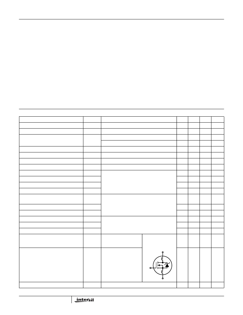
Internal Drain Inductance
Measured From Drain
Lead, 2.0mm (0.08in) From
Package to Center of Die
Modified MOSFET
Symbol Showing the
Internal Device
Inductances
-
4.0
-
nH
Internal Source Inductance
L
S
Measured From the Source
Lead, 2.0mm (0.08in) from
Package to Source
Bonding Pad
-
6.0
-
nH
Thermal Resistance, Junction to Ambient
R
θ
JA
Free Air Operation
-
-
120
o
C/W
L
S
L
D
G
D
S
IRFD310
相关PDF资料 |
PDF描述 |
|---|---|
| IRFD420 | Power MOSFET(Vdss=500V, Rds(on)=3.0ohm, Id=0.37A) |
| IRFD9020 | HEXFET TRANSISTORS P CHANNEL HEXDIP |
| IRFD9022 | HEXFET TRANSISTORS P CHANNEL HEXDIP |
| IRFD9120 | 1.0A, 100V, 0.6 Ohm, P-Channel Power MOSFET(1.0A, 100V, 0.6 Ω, P沟道功率MOS场效应管) |
| IRFD9220 | 0.6A, 200V, 1.500 Ohm, P-Channel Power MOSFET |
相关代理商/技术参数 |
参数描述 |
|---|---|
| IRFD310PBF | 功能描述:MOSFET N-Chan 400V 0.35 Amp RoHS:否 制造商:STMicroelectronics 晶体管极性:N-Channel 汲极/源极击穿电压:650 V 闸/源击穿电压:25 V 漏极连续电流:130 A 电阻汲极/源极 RDS(导通):0.014 Ohms 配置:Single 最大工作温度: 安装风格:Through Hole 封装 / 箱体:Max247 封装:Tube |
| IRFD310R | 制造商:未知厂家 制造商全称:未知厂家 功能描述:TRANSISTOR | MOSFET | N-CHANNEL | 400V V(BR)DSS | 400MA I(D) | TO-250VAR |
| IRFD311 | 制造商:Rochester Electronics LLC 功能描述:- Bulk |
| IRFD311R | 制造商:未知厂家 制造商全称:未知厂家 功能描述:TRANSISTOR | MOSFET | N-CHANNEL | 350V V(BR)DSS | 400MA I(D) | TO-250VAR |
| IRFD312 | 制造商:未知厂家 制造商全称:未知厂家 功能描述:TRANSISTOR | MOSFET | N-CHANNEL | 400V V(BR)DSS | 300MA I(D) | TO-250VAR |
发布紧急采购,3分钟左右您将得到回复。