参数资料
| 型号: | ISL32485EIBZ-T7A |
| 厂商: | Intersil |
| 文件页数: | 13/17页 |
| 文件大小: | 0K |
| 描述: | IC TXRX RS485 FAULT PROT 8SOIC |
| 产品培训模块: | Solutions for Industrial Control Applications |
| 标准包装: | 250 |
| 类型: | 收发器 |
| 驱动器/接收器数: | 1/1 |
| 规程: | RS422,RS485 |
| 电源电压: | 4.5 V ~ 5.5 V |
| 安装类型: | 表面贴装 |
| 封装/外壳: | 8-SOIC(0.154",3.90mm 宽) |
| 供应商设备封装: | 8-SOIC |
| 包装: | 带卷 (TR) |
ISL32483E, ISL32485E
5
FN7785.1
March 27, 2012
Absolute Maximum Ratings
Thermal Information
VCC to Ground . . . . . . . . . . . . . . . . . . . . . . . . . . . . . . . . . . . . . . . . . . . . . . . 7V
Input Voltages
DI, INV, RINV, DINV, DE, RE. . . . . . . . . . . . . . . . . . . . -0.3V to (VCC + 0.3V)
Input/Output Voltages
A/Y, B/Z, A, B, Y, Z. . . . . . . . . . . . . . . . . . . . . . . . . . . . . . . . . . . . . . . . ±60V
A/Y, B/Z, A, B, Y, Z
(Transient Pulse Through 100, see Note 15). . . . . . . . . . . . . . . . . ±80V
RO . . . . . . . . . . . . . . . . . . . . . . . . . . . . . . . . . . . . . . . . . -0.3V to (VCC +0.3V)
Short Circuit Duration
Y, Z. . . . . . . . . . . . . . . . . . . . . . . . . . . . . . . . . . . . . . . . . . . . . . . . . . Indefinite
ESD Rating . . . . . . . . . . . . . . . . . . . . see “ESD PERFORMANCE” on page 6
Latch-up (Tested per JESD78, Level 2, Class A). . . . . . . . . . . . . . . . +125°C
Thermal Resistance (Typical)
θJA (°C/W) θJC (°C/W)
8 Ld SOIC Package (Notes 4, 5). . . . . . . . . .
108
47
14 Ld SOIC Package (Notes 4, 5) . . . . . . . .
88
39
Maximum Junction Temperature (Plastic Package) . . . . . . . . . . . . +150°C
Maximum Storage Temperature Range . . . . . . . . . . . . . . -65°C to +150°C
Pb-free Reflow Profile . . . . . . . . . . . . . . . . . . . . . . . . . . . . . . . see link below
Recommended Operating Conditions
Supply Voltage (VCC) . . . . . . . . . . . . . . . . . . . . . . . . . . . . . . . . . . . . . . . . . . 5V
Temperature Range. . . . . . . . . . . . . . . . . . . . . . . . . . . . . . . . -40°C to +85°C
Bus Pin Common Mode Voltage Range . . . . . . . . . . . . . . . . . -25V to +25V
CAUTION: Do not operate at or near the maximum ratings listed for extended periods of time. Exposure to such conditions may adversely impact product
reliability and result in failures not covered by warranty.
NOTES:
4.
θJA is measured with the component mounted on a high effective thermal conductivity test board in free air. See Tech Brief TB379 for details.
5. For
θJC, the “case temp” location is taken at the package top center.
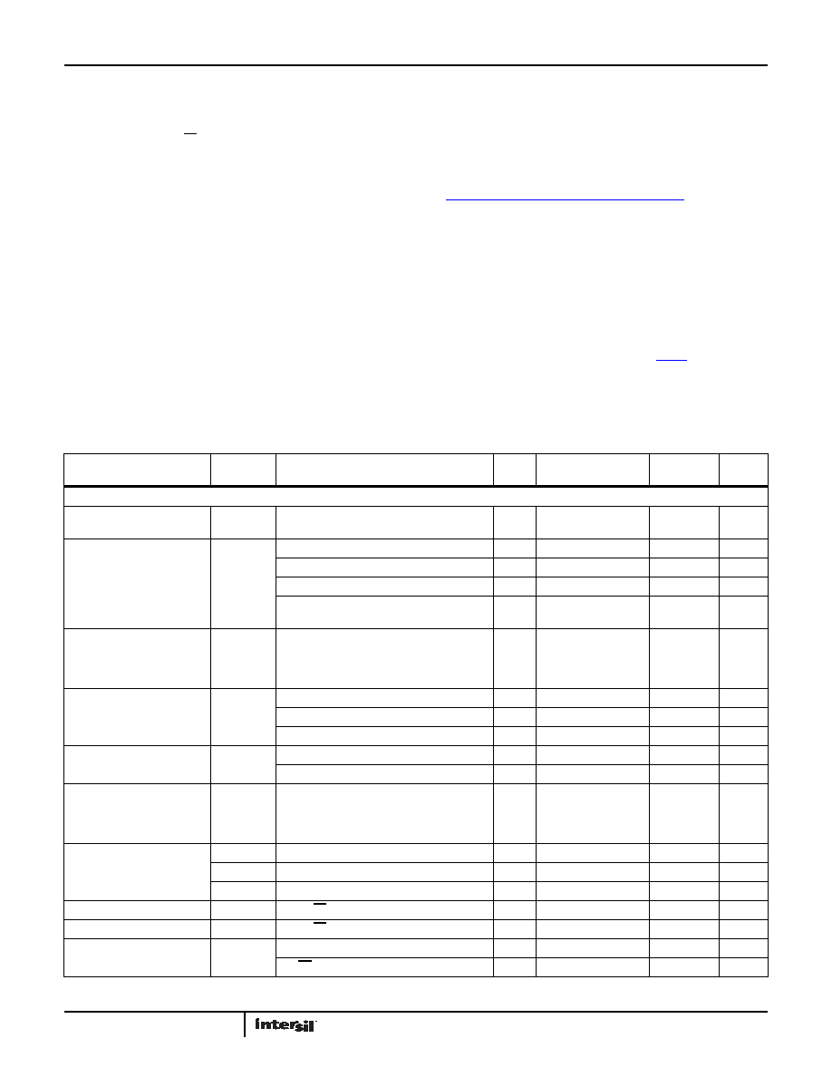
Electrical Specifications Test Conditions: VCC = 4.5V to 5.5V; Unless Otherwise Specified. Typicals are at VCC = 5V, TA = +25°C (Note 6).
Boldface limits apply over the operating temperature range, -40°C to +85°C.
PARAMETER
SYMBOL
TEST CONDITIONS
TEMP
(°C)
MIN
(Note 14)
TYP
MAX
(Note 14)
UNITS
DC CHARACTERISTICS
Driver Differential VOUT
(No load)
VOD1
Full
-
VCC
V
Driver Differential VOUT
(Loaded, Figure 3A)
VOD2
RL = 100 (RS-422)
Full
2.4
3.2
-
V
RL = 54 (RS-485)
Full
1.5
2.5
VCC
V
RL = 54 (PROFIBUS, VCC ≥ 5V)
Full
2.0
2.5
-
V
RL = 21 (Six 120 terminations for Star
Configurations, VCC ≥ 4.75V)
Full
0.8
1.3
-
V
Change in Magnitude of Driver
Differential VOUT for
Complementary Output
States
ΔVOD
Full
-
0.2
V
Driver Differential VOUT with
Common Mode Load
(Figure 3B)
VOD3
RL = 60, -7V ≤ VCM ≤ 12V
Full
1.5
2.1
VCC
V
RL = 60, -25V ≤ VCM ≤ 25V (VCC ≥ 4.75V)
Full
1.7
2.3
V
RL = 21, -15V ≤ VCM ≤ 15V (VCC ≥ 4.75V)
Full
0.8
1.1
-
V
Driver Common-Mode VOUT
(Figure 3)
VOC
RL = 54 or 100
Full
-1
-
3
V
RL = 60 or 100, -20V ≤ VCM ≤ 20V
Full
-2.5
-
5
V
Change in Magnitude of Driver
Common-Mode VOUT for
Complementary Output
States
DVOC
Full
-
0.2
V
Driver Short-Circuit Current
IOSD
Full
-250
-
250
mA
IOSD1
At First Fold-back, 22V ≤ VO ≤ -22V
Full
-83
83
mA
IOSD2
At Second Fold-back, 35V ≤ VO ≤ -35V
Full
-13
13
mA
Logic Input High Voltage
VIH
DE, DI, RE, INV, RINV, DINV
Full
2.5
-
V
Logic Input Low Voltage
VIL
DE, DI, RE, INV, RINV, DINV
Full
-
0.8
V
Logic Input Current
IIN1
DI
Full
-1
-
1
A
DE, RE, INV, RINV, DINV
Full
-15
6
15
A
相关PDF资料 |
PDF描述 |
|---|---|
| VE-J3P-MX-F4 | CONVERTER MOD DC/DC 13.8V 75W |
| V300A48T500BF3 | CONVERTER MOD DC/DC 48V 500W |
| VE-J3J-MX-F1 | CONVERTER MOD DC/DC 36V 75W |
| MS27466E15B68P | CONN RCPT 8POS WALL MT W/PINS |
| V300A48T500BF | CONVERTER MOD DC/DC 48V 500W |
相关代理商/技术参数 |
参数描述 |
|---|---|
| ISL32490E | 制造商:INTERSIL 制造商全称:Intersil Corporation 功能描述:±60V Fault Protected, 5V, RS-485/RS-422 Transceivers with ±25V CMR |
| ISL32490E-98E | 制造商:INTERSIL 制造商全称:Intersil Corporation 功能描述:Add a Loss of Signal (LOS) Indicator to Your RS-485 or RS-422 Transceiver |
| ISL32490EIBZ | 功能描述:IC TXRX RS485 FAULT PROT 14SOIC RoHS:是 类别:集成电路 (IC) >> 接口 - 驱动器,接收器,收发器 系列:- 产品培训模块:Lead (SnPb) Finish for COTS Obsolescence Mitigation Program 标准包装:50 系列:- 类型:收发器 驱动器/接收器数:1/1 规程:RS422,RS485 电源电压:4.75 V ~ 5.25 V 安装类型:通孔 封装/外壳:8-DIP(0.300",7.62mm) 供应商设备封装:8-PDIP 包装:管件 产品目录页面:1402 (CN2011-ZH PDF) |
| ISL32490EIBZ-T | 功能描述:IC TXRX RS485 FAULT PROT 14SOIC RoHS:是 类别:集成电路 (IC) >> 接口 - 驱动器,接收器,收发器 系列:- 产品培训模块:Lead (SnPb) Finish for COTS Obsolescence Mitigation Program 标准包装:2,500 系列:- 类型:发射器 驱动器/接收器数:4/0 规程:RS422,RS485 电源电压:4.75 V ~ 5.25 V 安装类型:表面贴装 封装/外壳:16-SOIC(0.154",3.90mm 宽) 供应商设备封装:16-SOIC 包装:带卷 (TR) |
| ISL32490EIBZ-T7A | 功能描述:RS-422/RS-485 接口 IC 14LD OVP -40+85 5V FL DUP 250KBPS TRANS RoHS:否 制造商:Maxim Integrated 数据速率:1136 Kbps 工作电源电压:3 V to 5.5 V 电源电流:5.9 mA 工作温度范围:- 40 C to + 85 C 安装风格:SMD/SMT 封装 / 箱体:SOIC-28 封装:Tube |
发布紧急采购,3分钟左右您将得到回复。