- 您现在的位置:买卖IC网 > PDF目录177785 > LCMXO1200E-4B256I (LATTICE SEMICONDUCTOR CORP) PDF资料下载
参数资料
| 型号: | LCMXO1200E-4B256I |
| 厂商: | LATTICE SEMICONDUCTOR CORP |
| 元件分类: | PLD |
| 中文描述: | FLASH PLD, 4.4 ns, PBGA256 |
| 封装: | 14 X 14 MM, CABGA-256 |
| 文件页数: | 17/96页 |
| 文件大小: | 1389K |
| 代理商: | LCMXO1200E-4B256I |
第1页第2页第3页第4页第5页第6页第7页第8页第9页第10页第11页第12页第13页第14页第15页第16页当前第17页第18页第19页第20页第21页第22页第23页第24页第25页第26页第27页第28页第29页第30页第31页第32页第33页第34页第35页第36页第37页第38页第39页第40页第41页第42页第43页第44页第45页第46页第47页第48页第49页第50页第51页第52页第53页第54页第55页第56页第57页第58页第59页第60页第61页第62页第63页第64页第65页第66页第67页第68页第69页第70页第71页第72页第73页第74页第75页第76页第77页第78页第79页第80页第81页第82页第83页第84页第85页第86页第87页第88页第89页第90页第91页第92页第93页第94页第95页第96页
2-21
Architecture
Lattice Semiconductor
MachXO Family Data Sheet
the system. These capabilities make the MachXO ideal for many multiple power supply and hot-swap applica-
tions.
Sleep Mode
The MachXO “C” devices (VCC = 1.8/2.5/3.3V) have a sleep mode that allows standby current to be reduced dra-
matically during periods of system inactivity. Entry and exit to Sleep mode is controlled by the SLEEPN pin.
During Sleep mode, the logic is non-operational, registers and EBR contents are not maintained, and I/Os are tri-
stated. Do not enter Sleep mode during device programming or configuration operation. In Sleep mode, power sup-
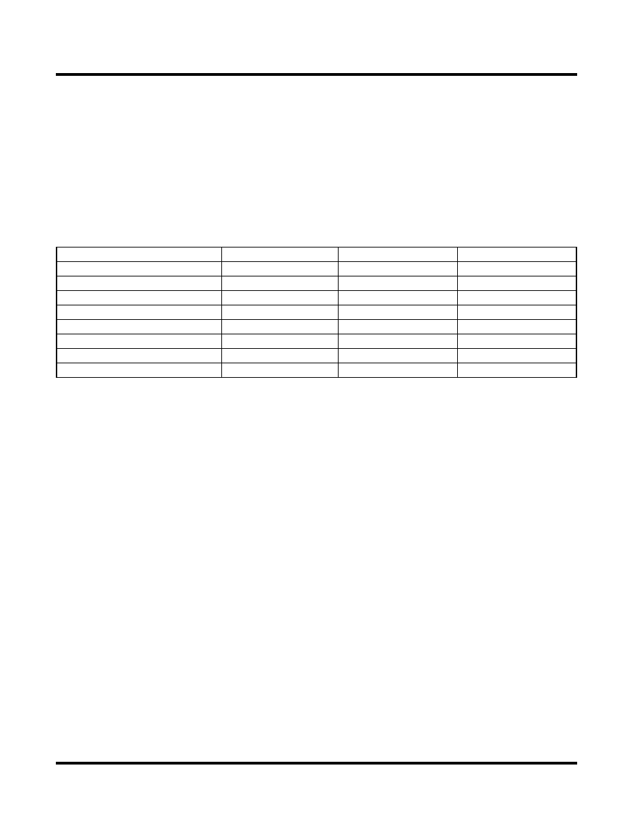
plies are in their normal operating range, eliminating the need for external switching of power supplies. Table 2-11
compares the characteristics of Normal, Off and Sleep modes.
Table 2-11. Characteristics of Normal, Off and Sleep Modes
SLEEPN Pin Characteristics
The SLEEPN pin behaves as an LVCMOS input with the voltage standard appropriate to the VCC supply for the
device. This pin also has a weak pull-up, along with a Schmidt trigger and glitch filter to prevent false triggering. An
external pull-up to VCC is recommended when Sleep Mode is not used to ensure the device stays in normal oper-
ation mode. Typically, the device enters sleep mode several hundred nanoseconds after SLEEPN is held at a valid
low and restarts normal operation as specified in the Sleep Mode Timing table. The AC and DC specifications por-
tion of this data sheet shows a detailed timing diagram.
Oscillator
Every MachXO device has an internal CMOS oscillator. The oscillator can be routed as an input clock to the clock
tree or to general routing resources. The oscillator frequency can be divided by internal logic. There is a dedicated
programming bit to enable/disable the oscillator. The oscillator frequency ranges from 18MHz to 26MHz.
Configuration and Testing
The following section describes the configuration and testing features of the MachXO family of devices.
IEEE 1149.1-Compliant Boundary Scan Testability
All MachXO devices have boundary scan cells that are accessed through an IEEE 1149.1 compliant test access
port (TAP). This allows functional testing of the circuit board, on which the device is mounted, through a serial scan
path that can access all critical logic nodes. Internal registers are linked internally, allowing test data to be shifted in
and loaded directly onto test nodes, or test data to be captured and shifted out for verification. The test access port
consists of dedicated I/Os: TDI, TDO, TCK and TMS. The test access port shares its power supply with one of the
VCCIO Banks (MachXO256: VCCIO1; MachXO640: VCCIO2; MachXO1200 and MachXO2280: VCCIO5) and can
operate with LVCMOS3.3, 2.5, 1.8, 1.5, and 1.2 standards.
For more details on boundary scan test, please see information regarding additional technical documentation at
the end of this data sheet.
Characteristic
Normal
Off
Sleep
SLEEPN Pin
High
—
Low
Static Icc
Typical <10mA
0
Typical <100uA
I/O Leakage
<10A
<1mA
<10A
Power Supplies VCC/VCCIO/VCCAUX
Normal Range
0
Normal Range
Logic Operation
User Defined
Non Operational
Non operational
I/O Operation
User Defined
Tri-state
JTAG and Programming circuitry
Operational
Non-operational
EBR Contents and Registers
Maintained
Non-maintained
相关PDF资料 |
PDF描述 |
|---|---|
| LCMXO1200C-3T144I | |
| LCMXO640E-4B256C | |
| LCMXO640E-3M132C | |
| LCMXO2280C-3T100I | |
| LCMXO1200C-3FT256I | |
相关代理商/技术参数 |
参数描述 |
|---|---|
| LCMXO1200E-4BN256C | 功能描述:CPLD - 复杂可编程逻辑器件 1200 LUTs 211 I/O 1.2V -4 SPD RoHS:否 制造商:Lattice 系列: 存储类型:EEPROM 大电池数量:128 最大工作频率:333 MHz 延迟时间:2.7 ns 可编程输入/输出端数量:64 工作电源电压:3.3 V 最大工作温度:+ 90 C 最小工作温度:0 C 封装 / 箱体:TQFP-100 |
| LCMXO1200E-4BN256I | 功能描述:CPLD - 复杂可编程逻辑器件 1200 LUTs 211 I/O 1.2V -4 SPD RoHS:否 制造商:Lattice 系列: 存储类型:EEPROM 大电池数量:128 最大工作频率:333 MHz 延迟时间:2.7 ns 可编程输入/输出端数量:64 工作电源电压:3.3 V 最大工作温度:+ 90 C 最小工作温度:0 C 封装 / 箱体:TQFP-100 |
| LCMXO1200E-4FT256C | 功能描述:CPLD - 复杂可编程逻辑器件 1200 LUTs 211 IO 1.2 V -4 Spd RoHS:否 制造商:Lattice 系列: 存储类型:EEPROM 大电池数量:128 最大工作频率:333 MHz 延迟时间:2.7 ns 可编程输入/输出端数量:64 工作电源电压:3.3 V 最大工作温度:+ 90 C 最小工作温度:0 C 封装 / 箱体:TQFP-100 |
| LCMXO1200E-4FT256I | 功能描述:CPLD - 复杂可编程逻辑器件 1200 LUTs 211 IO 1.2 V -4 Spd I RoHS:否 制造商:Lattice 系列: 存储类型:EEPROM 大电池数量:128 最大工作频率:333 MHz 延迟时间:2.7 ns 可编程输入/输出端数量:64 工作电源电压:3.3 V 最大工作温度:+ 90 C 最小工作温度:0 C 封装 / 箱体:TQFP-100 |
| LCMXO1200E-4FTN256C | 功能描述:CPLD - 复杂可编程逻辑器件 1200 LUTs 211 IO 1.2 V -4 Spd RoHS:否 制造商:Lattice 系列: 存储类型:EEPROM 大电池数量:128 最大工作频率:333 MHz 延迟时间:2.7 ns 可编程输入/输出端数量:64 工作电源电压:3.3 V 最大工作温度:+ 90 C 最小工作温度:0 C 封装 / 箱体:TQFP-100 |
发布紧急采购,3分钟左右您将得到回复。