- 您现在的位置:买卖IC网 > PDF目录378649 > LF48908QC31 (LOGIC DEVICES INC) Two Dimensional Convolver PDF资料下载
参数资料
| 型号: | LF48908QC31 |
| 厂商: | LOGIC DEVICES INC |
| 元件分类: | 数字信号处理外设 |
| 英文描述: | Two Dimensional Convolver |
| 中文描述: | 8-BIT, DSP-CONVOLVER, PQFP100 |
| 封装: | PLASTIC, QFP-100 |
| 文件页数: | 4/16页 |
| 文件大小: | 315K |
| 代理商: | LF48908QC31 |
DEVICES INCORPORATED
LF48908
Two Dimensional Convolver
4
Video Imaging Products
08/9/2000–LDS.48908-J
The filtered image data is output on
the Data Output bus (DOUT
19-0
). This
bus is registered with three-state
drivers to facilatate use on a standard
microprocessor system bus.
Data Input
Image data is input to the 3 x 3
convolver using DIN
7-0
. Data present
on DIN
7-0
is latched into a program-
mable pipeline delay on the rising
edge of CLK. The programmable
pipeline delay (1 to 4 clock cycles)
allows for synchronization of input
data when multiple LF48908s are
cascaded together to perform larger
convolutions. This delay is pro-
gramed via the Initialization Register
(see Table 3). The image data format,
unsigned or two’s complement, is also
controlled by this register.
Coefficient data is input to the 3 x 3
convolver using either of two Coef-
ficient Registers (CREG
0
or CREG
1
).
The Coefficient Registers are loaded
through CIN
7-0
using the A
2-0
, CS, and
LD controls. The coefficient data
format, unsigned or two’s comple-
ment, is determined by the Initializa-
tion Register.
Arithmetic Logic Unit
The input data path ALU with shifter
allows pixel point operations to be
performed on the incoming image.
These operations include arithmetic
functions, logical masking, and left/
right shifts. The 10-bit ALU Micro-
code Register controls the various
operations. The three upper bits
control the shift amount and direction
while the seven lower bits determine
the arithmetic or logical operation.
The shift operation is performed on
the output of the ALU. This shift
operation is independent of the
arithmetic or logical operation of the
ALU.
Tables 1 and 2 show the operations of
the ALU Microcode Register. The “A”
operand comes from the DIN input
data path, while the “B” operand is
taken from the ALU Register. The
ALU Register is loaded using CIN
7-0
and EALU. With EALU HIGH, data
from CIN
7-0
is loaded into the ALU
Register on the rising edge of CLK.
With EALU LOW, the data is held in
the ALU Register. Since CIN
7-0
is also
used to load the Control Logic Regis-
ters, it is possible to overwrite data in
those registers if CS and LD are active
when loading the ALU Register.
Therefore, special care must be taken
to ensure that CS and LD are not
active when writing to the ALU
Register.
Programmable Row Buffers
The two internal row buffers provide
the delay needed to perform the two-
dimensional convolution. The row
buffers function like 8-bit serial shift
registers with a user-programmable
delay from 1 to 1024 stages (it is
possible to select delay stages of 1 or
2, but this leads to meaningless results
for a 3 x 3 kernel convolution). The
row buffer length is set via the Row
Length Register (see Row Length
Register Section). The row buffers are
connected in series to provide the
proper pixel information to the
multiplier array. The Cascade Output
(CASO
7-0
) provides a 2X row delay of
the input data allowing for cascading
of LF48908s to handle larger frames
and/or kernel sizes. If more than 1024
delay stages are needed, it is possible
to use external row buffers and bypass
the internal row buffers. Bit 0 of the
Initialization Register determines if
internal or external row buffers are
used. If Bit 0 is a “0”, the internal row
buffers are used. If Bit 0 is a “1”, the
internal row buffers are bypassed and
external row buffers may be used.
3 x 3 Multiplier Array
The multiplier array comprises nine
8 x 8-bit multipliers. The active
Coefficient Register supplies the
coefficents to each of the multipliers,
while the pixel data comes from the
data input path and row buffers. The
array forms a sum-of-products result
as defined by the equation listed in
Figure 3.
CONTROL LOGIC
Four sets of registers, the ALU Micro-
code, Row Length, Initialization, and
Coefficient, define the Control Logic
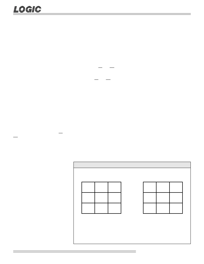
section. These registers are updated
F
IGURE
3.
M
ULTIPLIER
A
RRAY
O
UTPUT
P1
P2
P3
P4
P5
P6
P7
P8
P9
A
B
C
D
E
F
G
H
I
PIXEL INPUT DATA
FILTER KERNEL
MULTIPLIER ARRAY OUTPUT
A(P1)
=
+ D(P4)
+ G(P7)
+
+
+
B(P2)
E(P5)
H(P8)
+
+
+
C(P3)
F(P6)
I(P9)
相关PDF资料 |
PDF描述 |
|---|---|
| LF48908 | Two Dimensional Convolver |
| LF48908JC25 | Video Convolver |
| LF48908JC31 | Video Convolver |
| LF48908JC50 | Video Convolver |
| LF9501 | Programmable Line Buffer |
相关代理商/技术参数 |
参数描述 |
|---|---|
| LF48908QC50 | 制造商:未知厂家 制造商全称:未知厂家 功能描述:Video Convolver |
| LF48908QI25 | 制造商:未知厂家 制造商全称:未知厂家 功能描述:Video Convolver |
| LF48908QI31 | 制造商:未知厂家 制造商全称:未知厂家 功能描述:Video Convolver |
| LF48908QI50 | 制造商:未知厂家 制造商全称:未知厂家 功能描述:Video Convolver |
| LF4BK | 功能描述:PATCHCORD 1/4" BLACK 4FT RoHS:否 类别:电缆组件 >> 套管 - 音频 系列:LF 标准包装:1 系列:- 第一连接器:音频(RCA)插头 第二连接器:音频(RCA)插头 通道:单声 长度:15.0'(4.57m) 颜色:黑 屏蔽:- 使用:多媒体缆线 |
发布紧急采购,3分钟左右您将得到回复。