- 您现在的位置:买卖IC网 > PDF目录44981 > LT1507IS8#TR (LINEAR TECHNOLOGY CORP) 3 A SWITCHING REGULATOR, 570 kHz SWITCHING FREQ-MAX, PDSO8 PDF资料下载
参数资料
| 型号: | LT1507IS8#TR |
| 厂商: | LINEAR TECHNOLOGY CORP |
| 元件分类: | 稳压器 |
| 英文描述: | 3 A SWITCHING REGULATOR, 570 kHz SWITCHING FREQ-MAX, PDSO8 |
| 封装: | 0.150 INCH, PLASTIC, SO-8 |
| 文件页数: | 10/20页 |
| 文件大小: | 291K |
| 代理商: | LT1507IS8#TR |
18
LT1507
APPLICATIONS INFORMATION
WU
U
Example: with VIN = 5V, VOUT = 3.3V, IOUT = 1A;
P
W
PW
SW
BOOST
Q
=+
()
()( )
()
=+
=
+
=
=+
=
( . )( )( .)
..
.
(. )
..
(.
)
. (.
)
.
04 1 3 3
5
16 10
1 5 500 10
026 0 04
03
33
5
0 008
1
75
0 046
5 0 003
3 3 0 005
0 032
2
93
2
Total power dissipation is 0.3 + 0.046 + 0.032 = 0.38W.
Thermal resistance for the LT1507 packages is influenced
by the presence of internal or backside planes. With a full
plane under the SO package, thermal resistance will be
about 120
°C/W. No plane will increase resistance to about
150
°C/W. To calculate die temperature, use the proper
thermal resistance number for the desired package and
add in worst-case ambient temperature;
TJ = TA + θJA(PTOT)
With the S8 package (
θJA = 120°C/W) at an ambient
temperature of 70
°C;
TJ = 70 + 120(0.38) = 116°C
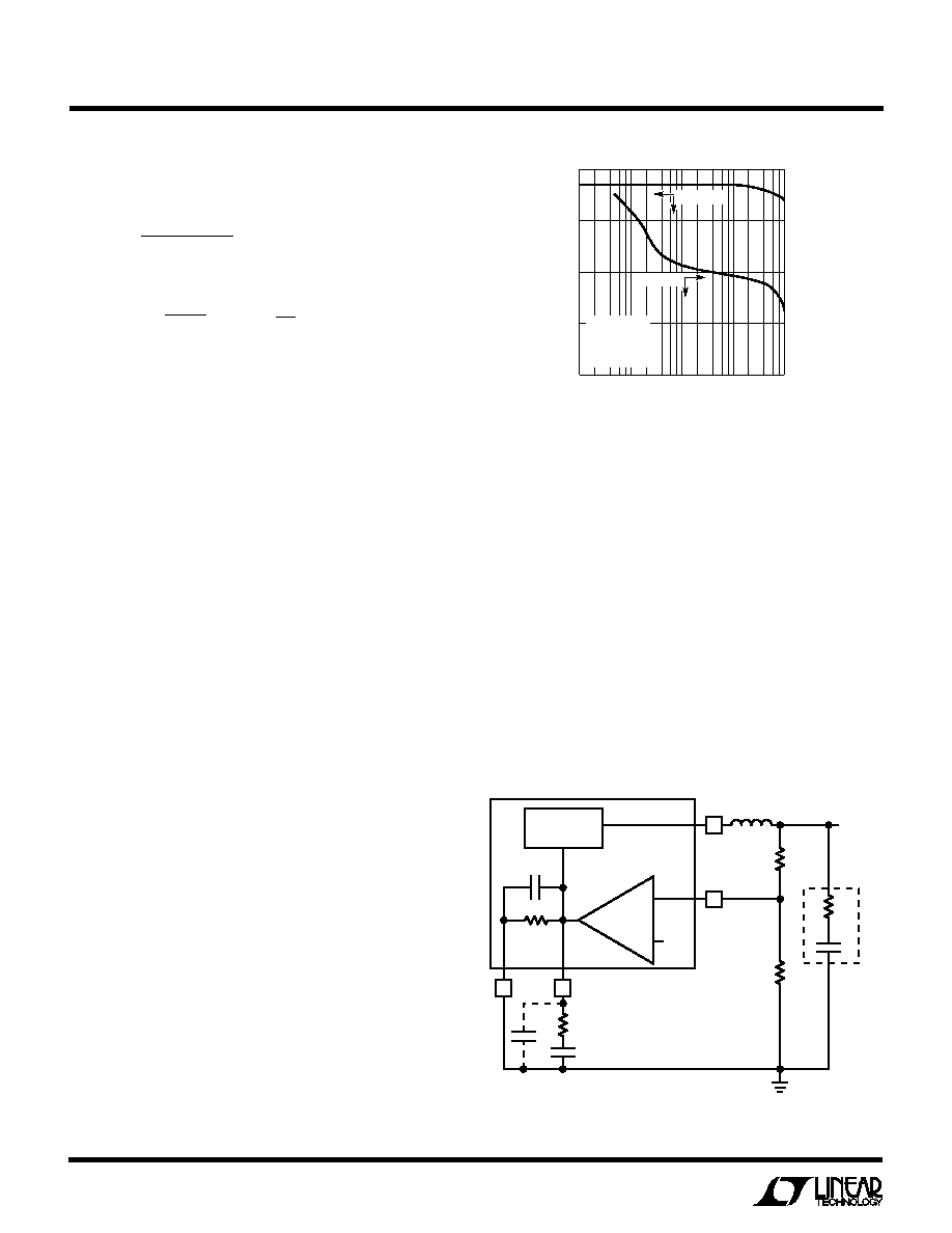
FREQUENCY COMPENSATION
The LT1507 uses a “current mode” architecture to help
alleviate phase shift created by the inductor. The basic
connections are shown in Figure 9. Gain of the power stage
can be modeled as 1.8A/V transconductance from the VC
pin voltage to current delivered to the output. This is
shown in Figure 8 where the transconductance from VC
pin to inductor current is essentially flat from 50Hz to
50kHz and phase shift is minimal in the important loop
unity-gain band of 1kHz to 50kHz. Inductor variation from
3
H to 20H will have very little effect on these curves.
Overall gain from the VC pin to output is then modeled as
the product of 1.8A/V transconductance multiplied by the
complex impedance of the load in parallel with the output
capacitor model.
The error amplifier can be modeled as a transconductance
of 2000
mho, with an output impedance of 200k in
FREQUENCY (Hz)
GAIN-V
C
PIN
TO
INDUCTOR
CURRENT
(A/V)
2.0
1.5
1.0
0.5
0
PHASE-V
C PIN
TO
INDUCTOR
CURRENT
(C
°
)
80
40
0
–40
–80
10
1k
10k
100k
LT1507 F08
100
GAIN (A/V)
PHASE
VOUT = 3.3V
IOUT = 250mA
VIN = 5V
L = 10
H
Figure 8. Phase and Gain from VC Pin Voltage
to Inductor Current
POWER STAGE
gm = 1.8A/V
ERROR AMPLIFIER
gm = 2000ho
200k
2.42V
LT1507
RC
CC
CF
GND
VC
VSW
L1
FB
R1
R2
ESR
+
OUTPUT
1507 F09
–
+
C1
12pF
Figure 9. Small-Signal Model for Loop Stability Analysis
parallel with 12pF. In all practical applications, the com-
pensation network from VC pin to ground has a much
lower impedance than the output impedance of the ampli-
fier at frequencies above 500Hz. This means that the error
amplifier characteristics themselves do not contribute
excess phase shift to the loop and the phase/gain charac-
teristics of the error amplifier section are completely
controlled by the external compensation network.
The complete small-signal model is shown in Figure 9. R1
and R2 are the divider used to set output voltage. These are
internal on the fixed voltage LT1507-3.3 with R1 = 1.8k
and R2 = 5k. RC, CC and CF are external compensation
相关PDF资料 |
PDF描述 |
|---|---|
| LT1507IS8-3.3#TR | 3 A SWITCHING REGULATOR, 570 kHz SWITCHING FREQ-MAX, PDSO8 |
| LT1509IS | 2 A POWER FACTOR CONTROLLER WITH POST REGULATOR, PDSO20 |
| LT1509CS | 2 A POWER FACTOR CONTROLLER WITH POST REGULATOR, PDSO20 |
| LT1513CT7 | 5.4 A BATTERY CHARGE CONTROLLER, 580 kHz SWITCHING FREQ-MAX, PZFM7 |
| LT1576IS8#TR | 3.5 A SWITCHING REGULATOR, 240 kHz SWITCHING FREQ-MAX, PDSO8 |
相关代理商/技术参数 |
参数描述 |
|---|---|
| LT1508 | 制造商:LINER 制造商全称:Linear Technology 功能描述:Power Factor and PWM Controller(Voltage Mode) |
| LT1508C | 制造商:LINER 制造商全称:Linear Technology 功能描述:Power Factor and PWM Controller(Voltage Mode) |
| LT1508CN | 制造商:LINER 制造商全称:Linear Technology 功能描述:Power Factor and PWM Controller(Voltage Mode) |
| LT1508CSW | 功能描述:IC PWM/POWER FACTOR CNTRLR20SOIC RoHS:否 类别:集成电路 (IC) >> PMIC - PFC(功率因数修正) 系列:- 产品培训模块:GreenChip Synchronous Rectification Control Family of ICs 标准包装:1 系列:- 模式:间歇导电(DCM) 频率 - 开关:- 电流 - 启动:- 电源电压:8.6 V ~ 38 V 工作温度:-20°C ~ 150°C 安装类型:表面贴装 封装/外壳:14-SOIC(0.154",3.90mm 宽) 供应商设备封装:14-SO 包装:Digi-Reel® 其它名称:568-5348-6 |
| LT1508I | 制造商:LINER 制造商全称:Linear Technology 功能描述:Power Factor and PWM Controller(Voltage Mode) |
发布紧急采购,3分钟左右您将得到回复。