- 您现在的位置:买卖IC网 > PDF目录14792 > LT3431EFE#PBF (Linear Technology)IC REG BUCK ADJ 3A 16TSSOP PDF资料下载
参数资料
| 型号: | LT3431EFE#PBF |
| 厂商: | Linear Technology |
| 文件页数: | 22/28页 |
| 文件大小: | 0K |
| 描述: | IC REG BUCK ADJ 3A 16TSSOP |
| 标准包装: | 95 |
| 类型: | 降压(降压) |
| 输出类型: | 可调式 |
| 输出数: | 1 |
| 输出电压: | 1.2 V ~ 48 V |
| 输入电压: | 5.5 V ~ 60 V |
| PWM 型: | 电流模式 |
| 频率 - 开关: | 500kHz |
| 电流 - 输出: | 3A |
| 同步整流器: | 无 |
| 工作温度: | -40°C ~ 125°C |
| 安装类型: | 表面贴装 |
| 封装/外壳: | 16-TSSOP(0.173",4.40mm)裸露焊盘 |
| 包装: | 管件 |
| 供应商设备封装: | 16-TSSOP-EP |
| 产品目录页面: | 1331 (CN2011-ZH PDF) |
第1页第2页第3页第4页第5页第6页第7页第8页第9页第10页第11页第12页第13页第14页第15页第16页第17页第18页第19页第20页第21页当前第22页第23页第24页第25页第26页第27页第28页
�� �
�
�LT3431�
�APPLICATIO� S� I� FOR� ATIO�
�tantalum� output� capacitor� with� a� ceramic� output� capacitor�
�because� of� its� very� low� ESR.� The� zero� provided� by� the�
�tantalum� output� capacitor� must� now� be� reinserted� back�
�into� the� loop.� Alternatively� there� may� be� cases� where,� even�
�with� the� tantalum� output� capacitor,� an� additional� zero� is�
�required� in� the� loop� to� increase� phase� margin� for� improved�
�transient� response.�
�A� zero� can� be� added� into� the� loop� by� placing� a� resistor,� R� C,�
�at� the� V� C� pin� in� series� with� the� compensation� capacitor,� C� C�
�or� by� placing� a� capacitor,� C� FB� ,� between� the� output� and� the�
�FB� pin.�
�a� capacitor,� C� FB� ,� can� be� inserted� between� the� output� and�
�FB� pin� but� care� must� be� taken� for� high� output� voltage�
�applications.� Sudden� shorts� to� the� output� can� create�
�unacceptably� large� negative� transients� on� the� FB� pin.�
�For� V� IN� -to-V� OUT� ratios� <4,� higher� loop� bandwidths� are�
�possible� by� readjusting� the� frequency� compensation� com-�
�ponents� at� the� V� C� pin.�
�When� checking� loop� stability,� the� circuit� should� be� oper-�
�ated� over� the� application’s� full� voltage,� current� and�
�temperature� range.� Proper� loop� compensation� may� be�
�obtained� by� empirical� methods� as� described� in� detail� in�
�80�
�60�
�40�
�GAIN�
�180�
�150�
�120�
�Application� Notes� 19� and� 76.�
�CONVERTER� WITH� BACKUP� OUTPUT� REGULATOR�
�20�
�0�
�–20�
�PHASE�
�90�
�60�
�30�
�In� systems� with� a� primary� and� backup� supply,� for� ex-�
�ample,� a� battery� powered� device� with� a� wall� adapter� input,�
�the� output� of� the� LT3431� can� be� held� up� by� the� backup�
�supply� with� the� LT3431� input� disconnected.� In� this� condi-�
�–40�
�10� 100� 1k� 10k� 100k�
�FREQUENCY� (Hz)�
�V� IN� =� 12V� R� C� =� 3.3k�
�V� OUT� =� 5V� C� C� =� 22nF�
�I� LOAD� =� 1A� C� F� =� 220pF�
�C� OUT� =� 100� μ� F,� 10V,� 0.1� ?�
�0�
�1M�
�3431� F11�
�tion,� the� SW� pin� will� source� current� into� the� V� IN� pin.� If� the�
�SHDN� pin� is� held� at� ground,� only� the� shut� down� current� of�
�30� μ� A� will� be� pulled� via� the� SW� pin� from� the� second� supply.�
�With� the� SHDN� pin� floating,� the� LT3431� will� consume� its�
�Figure� 11.� Overall� Loop� Response�
�When� using� R� C� ,� the� maximum� value� has� two� limitations.�
�First,� the� combination� of� output� capacitor� ESR� and� R� C� may�
�stop� the� loop� rolling� off� altogether.� Second,� if� the� loop� gain�
�is� not� rolled� sufficiently� at� the� switching� frequency,� output�
�ripple� will� perturb� the� V� C� pin� enough� to� cause� unstable�
�quiescent� operating� current� of� 1.5mA.� The� V� IN� pin� will� also�
�source� current� to� any� other� components� connected� to� the�
�input� line.� If� this� load� is� greater� than� 10mA� or� the� input�
�could� be� shorted� to� ground,� a� series� Schottky� diode� must�
�be� added,� as� shown� in� Figure� 12.� With� these� safeguards,�
�the� output� can� be� held� at� voltages� up� to� the� V� IN� absolute�
�maximum� rating.�
�duty� cycle� switching� similar� to� subharmonic� oscillation.� If�
�needed,� an� additional� capacitor� (C� F� )� can� be� added� across�
�the� R� C� /C� C� network� from� V� C� pin� to� ground� to� further�
�suppress� V� C� ripple� voltage.�
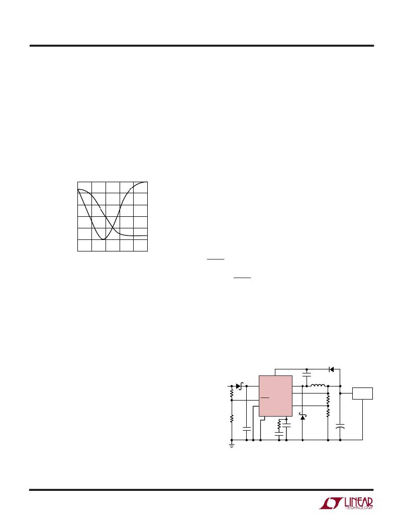
�With� a� tantalum� output� capacitor,� the� LT3431� already�
�REMOVABLE�
�INPUT�
�D3�
�30BQ060�
�54k�
�V� IN�
�SHDN�
�BOOST�
�LT3431�
�SW�
�BIAS�
�D2�
�MMSD914TI�
�C2�
�0.22� μ� F�
�10� μ� H�
�R1�
�15.4k�
�5V,� 2A� ALTERNATE�
�SUPPLY�
�includes� a� resistor,� R� C� and� filter� capacitor,� C� F� ,� at� the� V� C� pin�
�(see� Figures� 10� and� 11)� to� compensate� the� loop� over� the�
�entire� V� IN� range� (to� allow� for� stable� pulse� skipping� for� high�
�V� IN� -to-V� OUT� ratios� ≥� 4).� A� ceramic� output� capacitor� can� still�
�25k�
�C3�
�4.7� μ� F�
�SYNC�
�GND�
�R� C�
�3.3k�
�C� C�
�0.022� μ� F�
�FB�
�V� C�
�C� F�
�220pF�
�D1�
�30BQ060�
�R2�
�4.99k�
�+�
�C1�
�100� μ� F�
�10V�
�3431� F12�
�be� used� with� a� simple� adjustment� to� the� resistor� R� C� for�
�stable� operation.� (See� Ceramic� Capacitors� section� for�
�stabilizing� LT3431).� If� additional� phase� margin� is� required,�
�Figure� 12.� Dual� Source� Supply� with� 25� μ� A� Reverse� Leakage�
�sn3431� 3431fs�
�22�
�相关PDF资料 |
PDF描述 |
|---|---|
| SRP1205-7R2Y | INDUCTOR 7.2UH 8.3A SMD |
| SRP1205-5R6Y | INDUCTOR 5.6UH 8.5A SMD |
| LT3430EFE#PBF | IC REG BUCK ADJ 3A 16TSSOP |
| SRP1205-4R0Y | INDUCTOR 4UH 10.5A SMD |
| SRP1205-3R3Y | INDUCTOR 3.3UH 11A SMD |
相关代理商/技术参数 |
参数描述 |
|---|---|
| LT3431IFE | 功能描述:IC REG BUCK ADJ 3A 16TSSOP RoHS:否 类别:集成电路 (IC) >> PMIC - 稳压器 - DC DC 开关稳压器 系列:- 设计资源:Design Support Tool 标准包装:1 系列:- 类型:升压(升压) 输出类型:固定 输出数:1 输出电压:3V 输入电压:0.75 V ~ 2 V PWM 型:- 频率 - 开关:- 电流 - 输出:100mA 同步整流器:是 工作温度:-40°C ~ 85°C 安装类型:表面贴装 封装/外壳:SOT-23-5 细型,TSOT-23-5 包装:剪切带 (CT) 供应商设备封装:TSOT-23-5 其它名称:AS1323-BTTT-30CT |
| LT3431IFE#PBF | 功能描述:IC REG BUCK ADJ 3A 16TSSOP RoHS:是 类别:集成电路 (IC) >> PMIC - 稳压器 - DC DC 开关稳压器 系列:- 产品培训模块:MIC23xxx HyperLight Load™ Regulators 标准包装:5,000 系列:HyperLight Load® 类型:降压(降压) 输出类型:固定 输出数:1 输出电压:1.8V 输入电压:2.7 V ~ 5.5 V PWM 型:混合物 频率 - 开关:4MHz 电流 - 输出:2A 同步整流器:是 工作温度:-40°C ~ 125°C 安装类型:表面贴装 封装/外壳:8-VFDFN 裸露焊盘,8-MLF? 包装:带卷 (TR) 供应商设备封装:8-MLF?(2x2) 产品目录页面:1094 (CN2011-ZH PDF) 其它名称:576-3303-2 |
| LT3431IFE#PBF | 制造商:Linear Technology 功能描述:IC STEP-DOWN REGULATOR 16-TSSOP 制造商:Linear Technology 功能描述:IC, STEP-DOWN REGULATOR, 16-TSSOP |
| LT3431IFE#TR | 功能描述:IC REG BUCK ADJ 3A 16TSSOP RoHS:否 类别:集成电路 (IC) >> PMIC - 稳压器 - DC DC 开关稳压器 系列:- 设计资源:Design Support Tool 标准包装:1 系列:- 类型:升压(升压) 输出类型:固定 输出数:1 输出电压:3V 输入电压:0.75 V ~ 2 V PWM 型:- 频率 - 开关:- 电流 - 输出:100mA 同步整流器:是 工作温度:-40°C ~ 85°C 安装类型:表面贴装 封装/外壳:SOT-23-5 细型,TSOT-23-5 包装:剪切带 (CT) 供应商设备封装:TSOT-23-5 其它名称:AS1323-BTTT-30CT |
| LT3431IFE#TRPBF | 功能描述:IC REG BUCK ADJ 3A 16TSSOP RoHS:是 类别:集成电路 (IC) >> PMIC - 稳压器 - DC DC 开关稳压器 系列:- 设计资源:Design Support Tool 标准包装:1 系列:- 类型:升压(升压) 输出类型:固定 输出数:1 输出电压:3V 输入电压:0.75 V ~ 2 V PWM 型:- 频率 - 开关:- 电流 - 输出:100mA 同步整流器:是 工作温度:-40°C ~ 85°C 安装类型:表面贴装 封装/外壳:SOT-23-5 细型,TSOT-23-5 包装:剪切带 (CT) 供应商设备封装:TSOT-23-5 其它名称:AS1323-BTTT-30CT |
发布紧急采购,3分钟左右您将得到回复。