- 您现在的位置:买卖IC网 > PDF目录14465 > LT3505IMS8E#PBF (Linear Technology)IC REG BUCK ADJ 1.2A 8MSOP PDF资料下载
参数资料
| 型号: | LT3505IMS8E#PBF |
| 厂商: | Linear Technology |
| 文件页数: | 10/24页 |
| 文件大小: | 0K |
| 描述: | IC REG BUCK ADJ 1.2A 8MSOP |
| 标准包装: | 50 |
| 类型: | 降压(降压) |
| 输出类型: | 可调式 |
| 输出数: | 1 |
| 输出电压: | 0.78 V ~ 33.8 V |
| 输入电压: | 3.6 V ~ 36 V |
| PWM 型: | 电流模式 |
| 频率 - 开关: | 200kHz ~ 3.01MHz |
| 电流 - 输出: | 1.2A |
| 同步整流器: | 无 |
| 工作温度: | -40°C ~ 125°C |
| 安装类型: | 表面贴装 |
| 封装/外壳: | 8-TSSOP,8-MSOP(0.118",3.00mm 宽)裸露焊盘 |
| 包装: | 管件 |
| 供应商设备封装: | 8-MSOP-EP |
�� �
�
�LT3505�
�APPLICATIONS� INFORMATION�
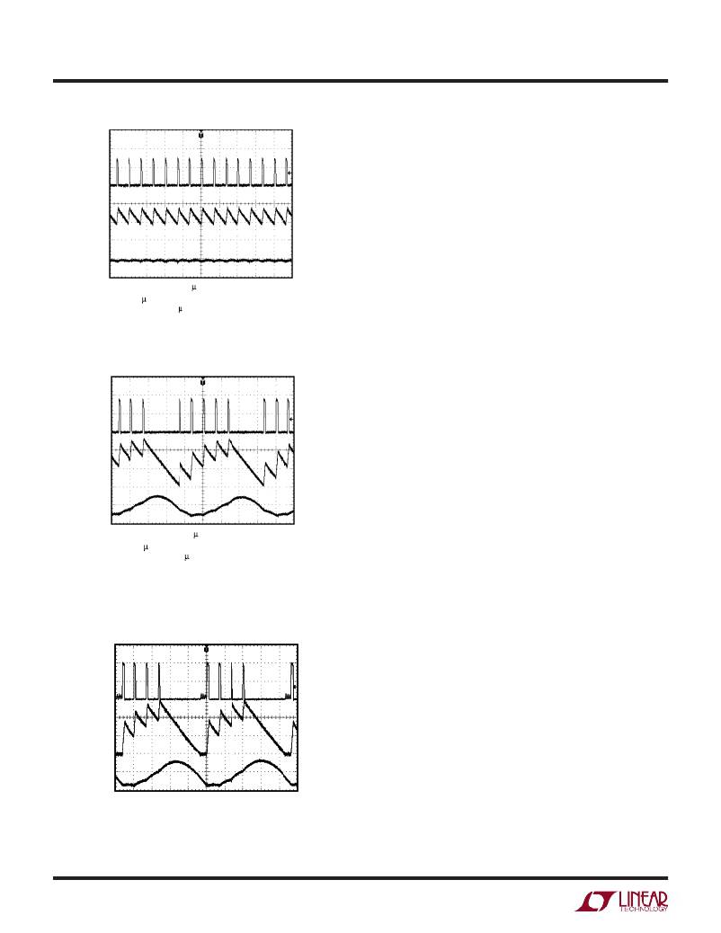
�V� SW�
�20V/DIV�
�I� L�
�0.5A/DIV�
�V� OUT�
�200mV/DIV�
�AC� COUPLED�
�Now� the� required� on� time� has� decreased� below� the�
�minimum� on� time� of� 130ns.� Instead� of� the� switch� pulse�
�width� becoming� narrower� to� accommodate� the� lower� duty�
�cycle� requirement,� the� switch� pulse� width� remains� ?xed�
�at� 130ns.� In� Figure� 2� the� inductor� current� ramps� up� to� a�
�value� exceeding� the� load� current� and� the� output� ripple�
�increases� to� ~200mV.� The� part� then� remains� off� until� the�
�output� voltage� dips� below� 100%� of� the� programmed� value�
�before� it� begins� switching� again.�
�V� SW�
�20V/DIV�
�I� L�
�0.5A/DIV�
�V� OUT�
�200mV/DIV�
�AC� COUPLED�
�2� s/DIV�
�C� OUT� =� 10� F� I� LOAD� =� 0.75A�
�V� OUT� =� 3V� L� =� 10� H�
�V� IN� =� 30V� R� T� =� 75.0k�
�Figure� 1�
�2� s/DIV�
�C� OUT� =� 10� F� I� LOAD� =� 0.75A�
�V� OUT� =� 3V� L� =� 10� H�
�V� IN� =� 35V� R� T� =� 75.0k�
�Figure� 2�
�3505� F01�
�3505� F02�
�For� switching� frequencies� above� 750kHz,� the� input� voltage�
�must� not� exceed� V� IN(PS)� .� See� the� “Input� Voltage� Frequency�
�Foldback”� section� of� the� datasheet� for� a� circuit� solution�
�that� provides� safe� operation� above� V� IN(PS)� at� switching�
�frequencies� exceeding� 750kHz.� For� switching� frequencies�
�below� 750kHz,� operation� above� V� IN(PS)� is� safe� and� will�
�not� damage� the� part� as� long� as� the� output� voltage� stays�
�in� regulation� and� the� inductor� does� not� saturate.� Figure�
�3� shows� the� switching� waveforms� of� a� 750kHz� applica-�
�tion� when� the� input� voltage� is� increased� to� its� absolute�
�maximum� rating� of� 40V.�
�As� the� input� voltage� increases,� the� inductor� current� ramp�
�rate� increases,� the� number� of� skipped� pulses� increases�
�and� the� output� voltage� ripple� increases.� The� part� is� robust�
�enough� to� survive� prolonged� operation� under� these� condi-�
�tions� as� long� as� the� programmed� switching� frequency� is�
�less� than� 750kHz� and� the� peak� inductor� current� does� not�
�exceed� 2.2A.� Inductor� current� saturation� may� further� limit�
�performance� in� this� operating� regime.�
�Frequency� Selection�
�V� SW�
�20V/DIV�
�I� L�
�0.5A/DIV�
�V� OUT�
�200mV/DIV�
�AC� COUPLED�
�2� μ� s/DIV�
�3505� F03�
�The� maximum� frequency� that� the� LT3505� can� be� pro-�
�grammed� to� is� 3MHz.� The� minimum� frequency� that� the�
�LT3505� can� be� programmed� to� is� 200kHz.� The� switching�
�frequency� is� programmed� by� tying� a� 1%� resistor� from� the� R� T�
�pin� to� ground.� Table� 1� can� be� used� to� select� the� value� of� R� T� .�
�Minimum� on-time� and� edge� loss� must� be� taken� into� consid-�
�eration� when� selecting� the� intended� frequency� of� operation.�
�Higher� switching� frequency� increases� power� dissipation�
�and� lowers� ef?ciency.�
�C� OUT� =� 10� μ� F�
�V� OUT� =� 3V�
�V� IN� =� 40V�
�I� LOAD� =� 0.75A�
�L� =� 10� μ� H�
�R� T� =� 75.0k�
�Figure� 3�
�3505fc�
�10�
�相关PDF资料 |
PDF描述 |
|---|---|
| LT1304CS8#PBF | IC REG BOOST ADJ 0.2A 8SOIC |
| RSM15DTMD-S189 | CONN EDGECARD 30POS R/A .156 SLD |
| LT1109CS8#PBF | IC REG BOOST ADJ 0.1A 8SOIC |
| HC2-R68TR-R | INDUCTOR PWR HI CURR 0.68UH SMD |
| VI-J5W-EX-B1 | CONVERTER MOD DC/DC 5.5V 75W |
相关代理商/技术参数 |
参数描述 |
|---|---|
| LT3505IMS8E-TR | 制造商:LINER 制造商全称:Linear Technology 功能描述:1.2A, Step-Down Switching Regulator in 3mm × 3mm DFN |
| LT3505IMS8E-TRPBF | 制造商:LINER 制造商全称:Linear Technology 功能描述:1.2A, Step-Down Switching Regulator in 3mm × 3mm DFN |
| LT3506 | 制造商:LINER 制造商全称:Linear Technology 功能描述:Monolithic Dual Tracking 3A Step-Down Switching |
| LT3506A | 制造商:LINER 制造商全称:Linear Technology 功能描述:Monolithic Dual Tracking 3A Step-Down Switching |
| LT3506AEDHD | 制造商:LINER 制造商全称:Linear Technology 功能描述:Dual Monolithic 1.6A Step-Down Switching Regulator |
发布紧急采购,3分钟左右您将得到回复。