- 您现在的位置:买卖IC网 > PDF目录44986 > LT3681EDE (LINEAR TECHNOLOGY CORP) 4.4 A SWITCHING REGULATOR, 3100 kHz SWITCHING FREQ-MAX, PDSO14 PDF资料下载
参数资料
| 型号: | LT3681EDE |
| 厂商: | LINEAR TECHNOLOGY CORP |
| 元件分类: | 稳压器 |
| 英文描述: | 4.4 A SWITCHING REGULATOR, 3100 kHz SWITCHING FREQ-MAX, PDSO14 |
| 封装: | 4 X 3 MM, PLASTIC, DFN-14 |
| 文件页数: | 6/24页 |
| 文件大小: | 367K |
| 代理商: | LT3681EDE |
LT3681
14
3681f
boost diode can be tied to VIN; however, this restricts the
input range to one-half of the absolute maximum rating
of the BOOST pin.
At light loads, the inductor current becomes discontinuous
and the effective duty cycle at the BOOST pin (not the SW
pin) can be very high. This reduces the minimum input
voltage to approximately 300mV above VOUT.Athigherload
currents, the inductor current is continuous and the duty
cycle is limited by the maximum duty cycle of the LT3681,
requiring a higher input voltage to maintain regulation.
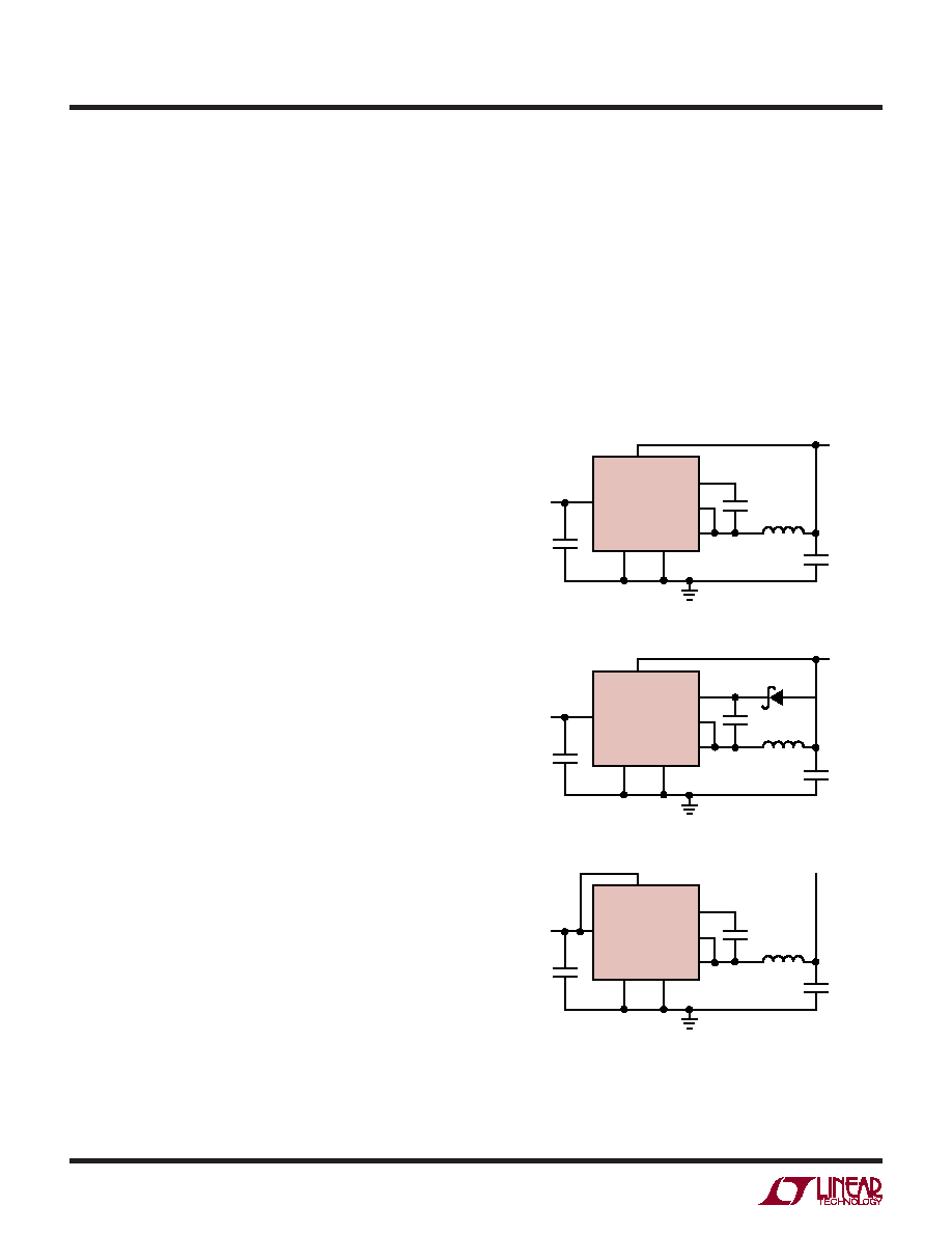
BOOST and BIAS Pin Considerations
Capacitor C3 and the internal boost Schottky diode (see
the Block Diagram) are used to generate a boost volt-
age that is higher than the input voltage. In most cases
a 0.22F capacitor will work well. Figure 5 shows three
ways to arrange the boost circuit. The BOOST pin must be
more than 2.3V above the SW pin for best efciency. For
outputs of 2.8V and above, the standard circuit (Figure 5a)
is best. For outputs between 2.8V and 3V, use a 1F boost
capacitor. A 2.5V output presents a special case because it
is marginally adequate to support the boosted drive stage
while using the internal boost diode. For reliable BOOST pin
operation with 2.5V outputs use a good external Schottky
diode (such as the ON Semi MBR0540), and a 1F boost
capacitor (see Figure 5b). For lower output voltages the
boost diode can be tied to the input (Figure 5c), or to
another supply greater than 2.8V. The circuit in Figure 5a
is more efcient because the BOOST pin current and BIAS
pin quiescent current comes from a lower voltage source.
You must also be sure that the maximum voltage ratings
of the BOOST and BIAS pins are not exceeded.
The minimum operating voltage of an LT3681 application
is limited by the minimum input voltage (3.6V) and by the
maximum duty cycle as outlined in a previous section. For
proper startup, the minimum input voltage is also limited
by the boost circuit. If the input voltage is ramped slowly,
or the LT3681 is turned on with its RUN/SS pin when the
output is already in regulation, then the boost capacitor
may not be fully charged. Because the boost capacitor is
charged with the energy stored in the inductor, the circuit
will rely on some minimum load current to get the boost
circuit running properly. This minimum load will depend
on input and output voltages, and on the arrangement of
the boost circuit. The minimum load generally goes to zero
once the circuit has started. If, however, the LT3681 is
started by the RUN/SS pin and the output is discharged, the
discharged output capacitance will often present enough
of a load to allow the circuit to start. Figure 6 gives plots
of the input voltage required for three different situations:
the worst case situation where RUN/SS is tied to VIN and
VIN is ramped up very slowly, the minimum input voltage
at which the circuit will regulate when start-up is controlled
by RUN/SS, and the minimum input voltage required to
maintain output regulation. For lower start-up voltage, the
VIN
BOOST
SW
BD
VIN
VOUT
4.7
mF
C3
GND
DC
LT3681
VIN
BOOST
SW
BD
VIN
VOUT
4.7
mF
C3
D2
GND
LT3681
VIN
BOOST
SW
BD
VIN
VOUT
4.7
mF
C3
GND
DA
LT3681
3681 FO5
COUT
(5a) For VOUT > 2.8V
(5b) For 2.5V < VOUT < 2.8V
(5c) For VOUT < 2.5V
DC
Figure 5. Three Circuits For Generating The Boost Voltage
APPLICATIONS INFORMATION
相关PDF资料 |
PDF描述 |
|---|---|
| LT3686AEMSE#PBF | 2.65 A SWITCHING REGULATOR, 2500 kHz SWITCHING FREQ-MAX, PDSO12 |
| LT3686AHMSE#TRPBF | 2.65 A SWITCHING REGULATOR, 2500 kHz SWITCHING FREQ-MAX, PDSO12 |
| LT3686AHMSE#PBF | 2.65 A SWITCHING REGULATOR, 2500 kHz SWITCHING FREQ-MAX, PDSO12 |
| LT3686AIMSE#TRPBF | 2.65 A SWITCHING REGULATOR, 2500 kHz SWITCHING FREQ-MAX, PDSO12 |
| LT3686AIDD#PBF | 2.65 A SWITCHING REGULATOR, 2500 kHz SWITCHING FREQ-MAX, PDSO10 |
相关代理商/技术参数 |
参数描述 |
|---|---|
| LT3681EDE#PBF | 功能描述:IC REG BUCK ADJ 2A 14DFN RoHS:是 类别:集成电路 (IC) >> PMIC - 稳压器 - DC DC 开关稳压器 系列:- 标准包装:250 系列:- 类型:降压(降压) 输出类型:固定 输出数:1 输出电压:1.2V 输入电压:2.05 V ~ 6 V PWM 型:电压模式 频率 - 开关:2MHz 电流 - 输出:500mA 同步整流器:是 工作温度:-40°C ~ 85°C 安装类型:表面贴装 封装/外壳:6-UFDFN 包装:带卷 (TR) 供应商设备封装:6-SON(1.45x1) 产品目录页面:1032 (CN2011-ZH PDF) 其它名称:296-25628-2 |
| LT3681EDE#PBF | 制造商:Linear Technology 功能描述:IC STEP-DOWN REGULATOR DFN-14 |
| LT3681EDE#TRPBF | 功能描述:IC REG BUCK ADJ 2A 14DFN RoHS:是 类别:集成电路 (IC) >> PMIC - 稳压器 - DC DC 开关稳压器 系列:- 设计资源:Design Support Tool 标准包装:1 系列:- 类型:升压(升压) 输出类型:固定 输出数:1 输出电压:3V 输入电压:0.75 V ~ 2 V PWM 型:- 频率 - 开关:- 电流 - 输出:100mA 同步整流器:是 工作温度:-40°C ~ 85°C 安装类型:表面贴装 封装/外壳:SOT-23-5 细型,TSOT-23-5 包装:剪切带 (CT) 供应商设备封装:TSOT-23-5 其它名称:AS1323-BTTT-30CT |
| LT3681EDEPBF | 制造商:Linear Technology 功能描述:36V 2.8MHz Step-Down Regulator LT3681 |
| LT3682 | 制造商:LINER 制造商全称:Linear Technology 功能描述:42V, 750mA Step-Down Regulator with 2.5μA |
发布紧急采购,3分钟左右您将得到回复。