- 您现在的位置:买卖IC网 > PDF目录10325 > LTC2499CUHF#TRPBF (Linear Technology)IC ADC 24BIT DELTA SIG 38-QFN PDF资料下载
参数资料
| 型号: | LTC2499CUHF#TRPBF |
| 厂商: | Linear Technology |
| 文件页数: | 18/34页 |
| 文件大小: | 0K |
| 描述: | IC ADC 24BIT DELTA SIG 38-QFN |
| 标准包装: | 2,500 |
| 位数: | 24 |
| 采样率(每秒): | 7.5 |
| 数据接口: | I²C,串行 |
| 转换器数目: | 1 |
| 功率耗散(最大): | 480µW |
| 电压电源: | 单电源 |
| 工作温度: | 0°C ~ 70°C |
| 安装类型: | 表面贴装 |
| 封装/外壳: | 38-WFQFN 裸露焊盘 |
| 供应商设备封装: | 38-QFN(5x7) |
| 包装: | 带卷 (TR) |
| 输入数目和类型: | 16 个单端,双极;8 个差分,双极 |
| 配用: | DC1012A-A-ND - BOARD DELTA SIGMA ADC LTC2499 |
第1页第2页第3页第4页第5页第6页第7页第8页第9页第10页第11页第12页第13页第14页第15页第16页第17页当前第18页第19页第20页第21页第22页第23页第24页第25页第26页第27页第28页第29页第30页第31页第32页第33页第34页
LTC2499
2499fd
(IIN+ – IIN–) is zero. While the differential input current is
zero, the common mode input current (IIN+ + IIN–)/2 is
proportional to the difference between the common mode
input voltage (VIN(CM)) and the common mode reference
voltage (VREF(CM)).
In applications where the input common mode voltage is
equal to the reference common mode voltage, as in the
case of a balanced bridge, both the differential and com-
mon mode input current are zero. The accuracy of the
converter is not compromised by settling errors.
In applications where the input common mode voltage is
constant but different from the reference common mode
voltage, the differential input current remains zero while
the common mode input current is proportional to the
difference between VIN(CM) and VREF(CM). For a reference
commonmodevoltageof2.5Vandaninputcommonmode
of 1.5V, the common mode input current is approximately
0.74A (in simultaneous 50Hz/60Hz rejection mode). This
commonmodeinputcurrentdoesnotdegradetheaccuracy
if the source impedances tied to IN+ and IN– are matched.
Mismatches in source impedance lead to a fixed offset
error but do not effect the linearity or full-scale reading.
A 1% mismatch in a 1k source resistance leads to a 74V
shift in offset voltage.
In applications where the common mode input voltage
varies as a function of the input signal level (single-ended
type sensors), the common mode input current varies
proportionally with input voltage. For the case of balanced
inputimpedances,thecommonmodeinputcurrenteffects
are rejected by the large CMRR of the LTC2499, leading
to little degradation in accuracy. Mismatches in source
impedances lead to gain errors proportional to the dif-
ference between the common mode input and common
mode reference. 1% mismatches in 1k source resistances
lead to gain errors on the order of 15ppm. Based on the
stability of the internal sampling capacitors and the ac-
curacy of the internal oscillator, a one-time calibration will
remove this error.
In addition to the input sampling current, the input ESD
protection diodes have a temperature dependent leakage
current. This current, nominally 1nA (±10nA max), results
in a small offset shift. A 1k source resistance will create a
1V typical and a 10V maximum offset voltage.
Automatic Offset Calibration of External Buffers/
Amplifiers
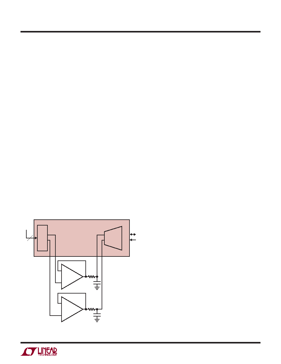
In addition to the Easy Drive input current cancellation,
the LTC2499 allows an external amplifier to be inserted
between the multiplexer output and the ADC input (see
Figure 12). This is useful in applications where balanced
source impedances are not possible. One pair of external
buffers/amplifiers can be shared between all 17 analog
inputs.TheLTC2499performsaninternaloffsetcalibration
every conversion cycle in order to remove the offset and
drift of the ADC. This calibration is performed through a
combination of front end switching and digital process-
ing. Since the external amplifier is placed between the
multiplexer and the ADC, it is inside this correction loop.
This results in automatic offset correction and offset drift
removal of the external amplifier.
The LTC6078 is an excellent amplifier for this function.
It operates with supply voltages as low as 2.7V and its
noise level is 18nV/√Hz. The Easy Drive input technology
of the LTC2499 enables an RC network to be added directly
to the output of the LTC6078. The capacitor reduces the
magnitude of the current spikes seen at the input to the
ADC and the resistor isolates the capacitor load from the
Figure 12. External Buffers Provide High Impedance Inputs
and Amplifier Offsets are Automatically Cancelled
applications inForMation
–
+
–
+
1/2 LTC6078
1
2
3
5
6
7
ADC
WITH
EASY DRIVE
INPUTS
INPUT
MUX
MUXOUTP
MUXOUTN
17
2499 F12
LTC2499
ANALOG
INPUTS
SCL
SDA
0.1F
1k
0.1F
相关PDF资料 |
PDF描述 |
|---|---|
| AD7887ARZ-REEL7 | IC ADC 12BIT 2CHAN SRL 8SOIC |
| LTC2498CUHF#TRPBF | IC ADC 24BIT 16CH 38-QFN |
| D38999/26WJ61PNLC | CONN HSG PLUG 61POS STRGHT PINS |
| LTC2430IGN#TRPBF | IC ADC 20BIT DIFFINPUT/REF16SSOP |
| LTC2435-1IGN#TRPBF | IC ADC DIFF I/REF 20BIT 16-SSOP |
相关代理商/技术参数 |
参数描述 |
|---|---|
| LTC2499IUHF#PBF | 功能描述:IC ADC 24BIT DELTA SIG 38-QFN RoHS:是 类别:集成电路 (IC) >> 数据采集 - 模数转换器 系列:- 标准包装:1 系列:microPOWER™ 位数:8 采样率(每秒):1M 数据接口:串行,SPI? 转换器数目:1 功率耗散(最大):- 电压电源:模拟和数字 工作温度:-40°C ~ 125°C 安装类型:表面贴装 封装/外壳:24-VFQFN 裸露焊盘 供应商设备封装:24-VQFN 裸露焊盘(4x4) 包装:Digi-Reel® 输入数目和类型:8 个单端,单极 产品目录页面:892 (CN2011-ZH PDF) 其它名称:296-25851-6 |
| LTC2499IUHF#TRPBF | 功能描述:IC ADC 24BIT DELTA SIG 38-QFN RoHS:是 类别:集成电路 (IC) >> 数据采集 - 模数转换器 系列:- 标准包装:1,000 系列:- 位数:16 采样率(每秒):45k 数据接口:串行 转换器数目:2 功率耗散(最大):315mW 电压电源:模拟和数字 工作温度:0°C ~ 70°C 安装类型:表面贴装 封装/外壳:28-SOIC(0.295",7.50mm 宽) 供应商设备封装:28-SOIC W 包装:带卷 (TR) 输入数目和类型:2 个单端,单极 |
| LTC2600CGN | 功能描述:IC DAC OCTAL R-R 16BIT 16SSOP RoHS:否 类别:集成电路 (IC) >> 数据采集 - 数模转换器 系列:- 产品培训模块:Data Converter Fundamentals DAC Architectures 标准包装:750 系列:- 设置时间:7µs 位数:16 数据接口:并联 转换器数目:1 电压电源:双 ± 功率耗散(最大):100mW 工作温度:0°C ~ 70°C 安装类型:表面贴装 封装/外壳:28-LCC(J 形引线) 供应商设备封装:28-PLCC(11.51x11.51) 包装:带卷 (TR) 输出数目和类型:1 电压,单极;1 电压,双极 采样率(每秒):143k |
| LTC2600CGN#PBF | 功能描述:IC DAC OCTAL R-R 16BIT 16SSOP RoHS:是 类别:集成电路 (IC) >> 数据采集 - 数模转换器 系列:- 产品培训模块:Lead (SnPb) Finish for COTS Obsolescence Mitigation Program 标准包装:50 系列:- 设置时间:4µs 位数:12 数据接口:串行 转换器数目:2 电压电源:单电源 功率耗散(最大):- 工作温度:-40°C ~ 85°C 安装类型:表面贴装 封装/外壳:8-TSSOP,8-MSOP(0.118",3.00mm 宽) 供应商设备封装:8-uMAX 包装:管件 输出数目和类型:2 电压,单极 采样率(每秒):* 产品目录页面:1398 (CN2011-ZH PDF) |
| LTC2600CGN#PBF | 制造商:Linear Technology 功能描述:IC 16BIT DAC OCTAL RR 16SSOP 制造商:Linear Technology 功能描述:IC, 16BIT DAC, OCTAL, RR, 16SSOP |
发布紧急采购,3分钟左右您将得到回复。