参数资料
| 型号: | LTC6360CDD#PBF |
| 厂商: | Linear Technology |
| 文件页数: | 4/24页 |
| 文件大小: | 0K |
| 描述: | IC ADC DRIVER TRUE ZERO 8DFN |
| 标准包装: | 121 |
| 类型: | ADC 驱动器 |
| 应用: | 数据采集 |
| 安装类型: | 表面贴装 |
| 封装/外壳: | 8-WFDFN 裸露焊盘 |
| 供应商设备封装: | 8-DFN(3x3) |
| 包装: | 管件 |
LTC6360
12
6360f
applicaTions inForMaTion
Amplifier Characteristics
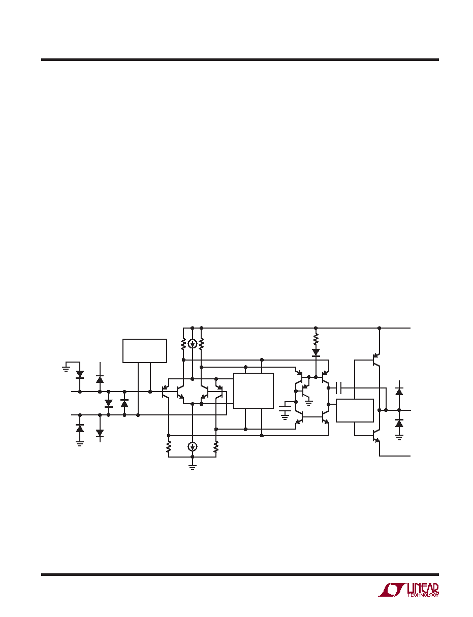
Figure 5 shows a simplified schematic of the LTC6360’s
amplifier. The input stage has NPN and PNP differential
pairs operating in parallel. This topology allows the inputs
to swing all the way from the negative rail to within 0.75V
of the positive supply rail. The PNP differential pair is
the primary input differential pair and is active when the
common mode voltage is less than 1.5V from the positive
rail. When the common mode voltage exceeds VCC – 1.5V,
the NPN pair is activated and the PNP is deactivated. The
input stage transconductance, gm, is maintained nearly
constant during the handover from PNP pair to NPN pair.
Additionally, a precision two-point trim algorithm is used
to maintain near constant offset voltage over the entire
input common mode range.
Input bias current flows out of the +IN and –IN inputs. The
magnitude of this current is regulated via an input current
compensation circuit which eliminates the discontinuity
and polarity reversal of input bias current that would oth-
erwise occur when transitioning from one input pair to the
other. Typical total change in input bias current over the
entire input common mode range is approximately 3.5A.
Amplifier Feedback Components
When feedback resistors are used to set gain, care should
be taken to ensure that the pole formed by the feedback
resistors and the total capacitance at the inverting input,
–IN, does not degrade stability. For instance, to set the
LTC6360 in a gain of +2, RF and RG of Figure 3 could be
set to 2k. If the total capacitance at –IN (LTC6360 plus
PC board) were 2pF, a new pole would be formed in the
loop response at 80MHz, which could lead to instability or
ringinginthestepresponse.Acapacitorconnectedacross
the feedback resistor and having the same value as the
total –IN parasitic capacitance will eliminate any ringing
or oscillation. Special care should be taken during layout,
including using the shortest possible trace lengths and
removing the ground plane under the –IN pin, to minimize
the parasitic capacitance.
Figure 5. Amplifier Simplified Schematic
6360 F05
VCC
CPI
OUT
DESD5
DESD6
VCC
DESD1
DESD2
+IN
–IN
DESD3
DESD4
D1
D2
INPUT
CURRENT
COMPENSATION
INPUT PAIR
CONTROL
DIFFERENTIAL
DRIVE
GENERATOR
相关PDF资料 |
PDF描述 |
|---|---|
| VI-J6N-MW-S | CONVERTER MOD DC/DC 18.5V 100W |
| LT1567IMS8#TR | IC BLOCK BUILD FLTR LONOIS 8MSOP |
| VI-J6L-MW-S | CONVERTER MOD DC/DC 28V 100W |
| LT1567IMS8#PBF | IC BLOCK BUILD FLTR LONOIS 8MSOP |
| AD7808BRZ-REEL | IC DAC 10BIT OCTAL SRL 24-SOIC |
相关代理商/技术参数 |
参数描述 |
|---|---|
| LTC6360CMS8E#PBF | 功能描述:IC ADC DRIVER TRUE ZERO 8-MSOP RoHS:是 类别:集成电路 (IC) >> 线性 - 放大器 - 专用 系列:- 产品培训模块:Lead (SnPb) Finish for COTS Obsolescence Mitigation Program 标准包装:60 系列:- 类型:可变增益放大器 应用:CATV 安装类型:表面贴装 封装/外壳:20-WQFN 裸露焊盘 供应商设备封装:20-TQFN-EP(5x5) 包装:托盘 |
| LTC6360CMS8E#TRPBF | 功能描述:IC ADC DRIVER TRUE ZERO 8MSOP RoHS:是 类别:集成电路 (IC) >> 线性 - 放大器 - 专用 系列:- 产品培训模块:Lead (SnPb) Finish for COTS Obsolescence Mitigation Program 标准包装:60 系列:- 类型:可变增益放大器 应用:CATV 安装类型:表面贴装 封装/外壳:20-WQFN 裸露焊盘 供应商设备封装:20-TQFN-EP(5x5) 包装:托盘 |
| LTC6360HDD#PBF | 功能描述:IC ADC DRIVER TRUE ZERO 8DFN RoHS:是 类别:集成电路 (IC) >> 线性 - 放大器 - 专用 系列:- 产品培训模块:Lead (SnPb) Finish for COTS Obsolescence Mitigation Program 标准包装:60 系列:- 类型:可变增益放大器 应用:CATV 安装类型:表面贴装 封装/外壳:20-WQFN 裸露焊盘 供应商设备封装:20-TQFN-EP(5x5) 包装:托盘 |
| LTC6360HDD#TRPBF | 功能描述:IC ADC DRIVER TRUE ZERO 8DFN RoHS:是 类别:集成电路 (IC) >> 线性 - 放大器 - 专用 系列:- 产品培训模块:Lead (SnPb) Finish for COTS Obsolescence Mitigation Program 标准包装:60 系列:- 类型:可变增益放大器 应用:CATV 安装类型:表面贴装 封装/外壳:20-WQFN 裸露焊盘 供应商设备封装:20-TQFN-EP(5x5) 包装:托盘 |
| LTC6360HMS8E#PBF | 功能描述:IC ADC DRIVER TRUE ZERO 8MSOP RoHS:是 类别:集成电路 (IC) >> 线性 - 放大器 - 专用 系列:- 产品培训模块:Lead (SnPb) Finish for COTS Obsolescence Mitigation Program 标准包装:60 系列:- 类型:可变增益放大器 应用:CATV 安装类型:表面贴装 封装/外壳:20-WQFN 裸露焊盘 供应商设备封装:20-TQFN-EP(5x5) 包装:托盘 |
发布紧急采购,3分钟左右您将得到回复。